Download (Size : 291.24KB)
2SJ3053DV mosfet equivalent, p-channel mosfet.
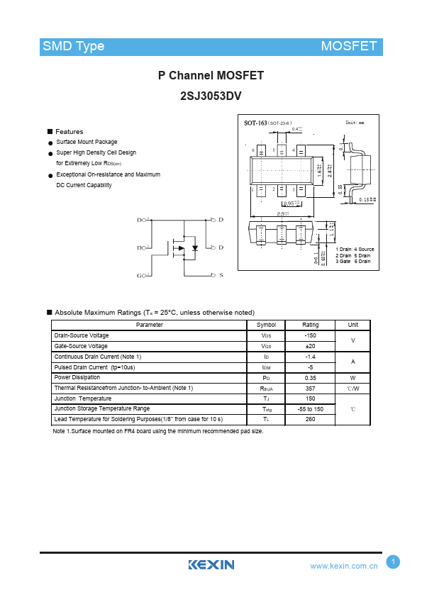
* Surface Mount Package * Super High Density Cell Design for Extremely Low RDS(on) * Exceptional On-resistance and Maximum DC Current Capability ( SOT-23-6 ).
Image gallery
TAGS
Manufacturer
Related datasheet
2SJ305
2SJ302
2SJ302-Z
2SJ302-ZJ
2SJ303
2SJ304
2SJ306
2SJ307
2SJ308
2SJ312
2SJ313
2SJ315
2SJ316

 Download (Size : 291.24KB)