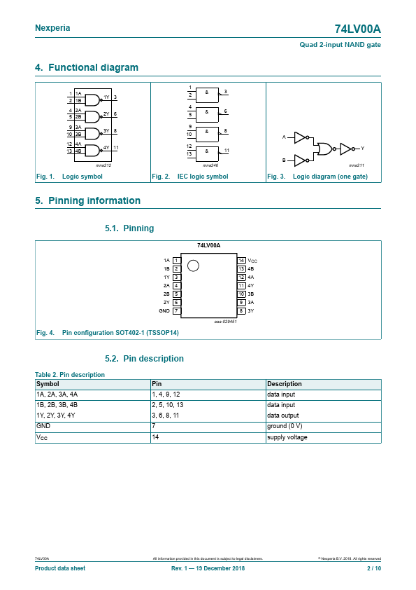
DatasheetsPDF.com

74LV00A

nexperia
Part Number 74LV00A
Manufacturer nexperia
Description Quad 2-input NAND gate
Published Jul 23, 2019
Detailed Description 74LV00A Quad 2-input NAND gate Rev. 1 — 19 December 2018 Product data sheet 1. General description The 74LV00A is a qu...
Datasheet PDF File 74LV00A PDF File

74LV00A
74LV00A


Overview
74LV00A Quad 2-input NAND gate Rev.
1 — 19 December 2018 Product data sheet 1.
General description The 74LV00A is a quad 2-input NAND gate.
Inputs are overvoltage tolerant.
This feature allows the use of these devices as translators in mixed voltage environments.
Schmitt-trigger action at all inputs makes the circuit tolerant of slower input rise and fall times.
This device is fully specified for partial power down applications using IOFF.
The IOFF circuitry disables the output, preventing the potentially damaging backflow current through the device when it is powered down.
2.
Features and benefits • Wide supply voltage range from 2.
0 V to 5.
5 V • Maximum tpd of 9 ns at 5 V • Typical VOL(p) < 0.
8 V at VCC = 3.
3 V, Tamb = 25 °C • Typical VOH(v) > 2.
3 V at VCC = 3.
3 V, Tamb = 25 °C • Supports mixed-mode voltage operation on all ports • IOFF circuitry provides partial Power-down mode operation • Latch-up performance exceeds 250 mA per JESD 78 Class II • ESD protection: • MM: MM JESD22-A115-B exceeds 200 V • HBM: ANSI/ESDA/JEDEC JS-001 Class 3A exceeds 4 kV • CDM: ANSI/ESDA/JEDEC JS-002 class C3 exceeds 2 kV • Specified from -40 °C to +85 °C and from -40 °C to +125 °C 3.
Ordering information Table 1.
Ordering information Type number Package Temperature range 74LV00APW -40 °C to +125 °C Name TSSOP14 Description plastic thin shrink small outline package; 14 leads; body width 4.
4 mm Version SOT402-1 Nexperia 4.
Functional diagram 1 1A 2 1B 4 2A 5 2B 9 3A 10 3B 12 4A 13 4B 1Y 3 2Y 6 3Y 8 4Y 11 mna212 Fig.
1.
Logic symbol 1 2& 3 4 5& 6 9 10 & 8 12 13 & 11 mna246 Fig.
2.
IEC logic symbol 5.
Pinning information 74LV00A Quad 2-input NAND gate A Y B mna211 Fig.
3.
Logic diagram (one gate) 5.
1.
Pinning 1A 1B 1Y 2A 2B 2Y GND 1 2 3 4 5 6 7 Fig.
4.
Pin configuration SOT402-1 (TSSOP14) 74LV00A 14 VCC 13 4B 12 4A 11 4Y 10 3B 9 3A 8 3Y aaa-029451 5.
2.
Pin description Table 2.
Pin description Symbol 1A, 2A, 3A, 4A 1B, 2B, 3B, 4B 1Y, 2Y, 3Y, 4Y GND VCC ...


Similar Datasheet


@ 2014 :: Datasheetspdf.com :: Semiconductors datasheet search & download site. (Privacy Policy & Contact)