STB200NF04L mosfet equivalent, n-channel stripfet ii mosfet.
TYPE STB200NF04L STP200NF04L STB200NF04L-1
s s s
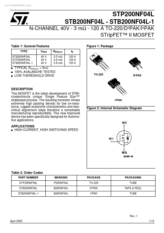
Figure 1: Package
RDS(on) 3.5 mΩ 3.8 mΩ 3.8 mΩ ID 120 A 120 A 120 A
3 1 2
VDSS 40 V 40 V 40 V
TYPICAL RDS(on) = 3mΩ 10.
APPLICATIONS s HIGH CURRENT, HIGH SWITCHING SPEED
3 12
I²PAK
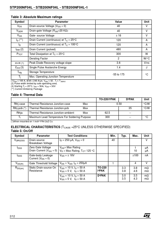
Figure 2: Internal Schematic Diagram
Table 2: Order Co.
This MOSFET is the latest development of STMicroelectronics unique “Single Feature Size™” stripbased process. The resulting transistor shows extremely high packing density for low on-resistance, rugged avalanche characteristics and lesscritical align.
Image gallery

TAGS
Manufacturer
Related datasheet
 Download (Size : 367.30KB)