M60006FP expander equivalent, 12-bit i/o expander.
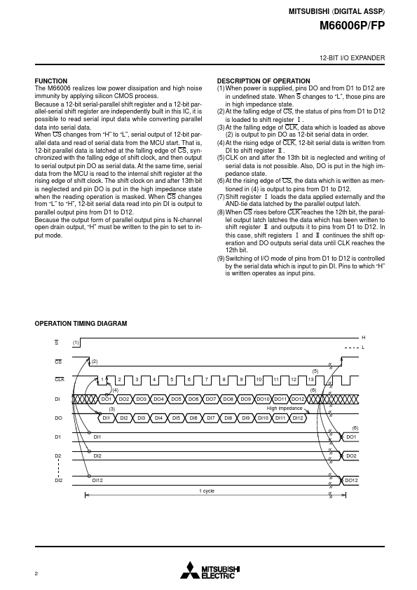
* Bi-directional serial data communication with MCU
* Read of serial data during parallel-serial conversion.
* Bit resolution of serial data I/O
* Low pow.
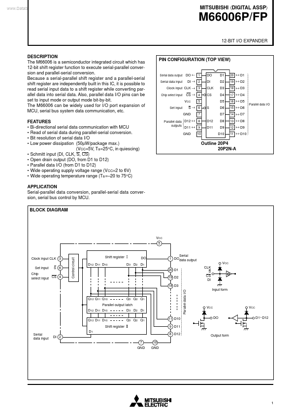
The M66006 is a semiconductor integrated circuit which has 12-bit shift register function to execute serial-parallel conversion and parallel-serial conversion. Because a serial-parallel shift register and a parallel-serial shift register are independ.
Image gallery

TAGS
 Download (Size : 101.13KB)