Search by part number and manufacturer or description
 File Size : 203.77KB
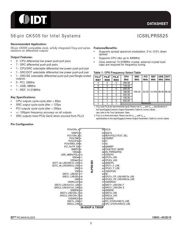
PIN # PIN NAME TYPE DESCRIPTION 3.3V PCI clock output or Clock Request control A for either SRC0 or SRC2 pair The power-up default is PCI0 output, but this pin may also be used as a Clock Request control of SRC pair 0 or SRC pair 2 via SMBus. Before configuring this pin as a Clock Request Pin, the P.
• 2 - CPU differential low power push-pull pairs
• 7 - SRC differential push-pull pairs
• 1 - CPU/SRC selectable differential low power push-pull pair
• 1 - SRC/DOT selectable differential low power push-pull pair
• 1 - SRC/SE selectable differential push-pull pair/Single-ended outputs
• 5 - PCI, 33MHz
• 1 - USB, 48MHz
• 1 - REF, 14.318MHz Key Specifications:
• CPU outputs cycle-cycle jitter < 85ps
• SRC output cycle-cycle jitter < 125ps
• PCI outputs cycle-cycle jitter < 250ps
• +/- 100ppm frequency accuracy on all outputs
• SRC outputs meet PCIe Gen2 when sourced from PLL3 Pin Configuration.


Similar Product