Search by part number and manufacturer or description
 File Size : 1.08MB
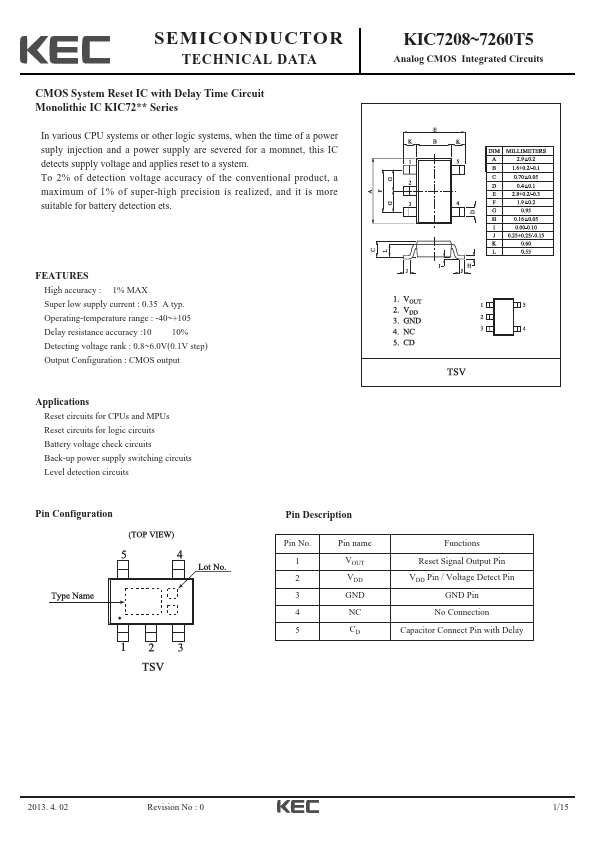
Pin No. 1 2 3 4 5 Pin name VOUT VDD GND NC CD Functions Reset Signal Output Pin VDD Pin / Voltage Detect Pin GND Pin No Connection Capacitor Connect Pin with Delay 2013. 4. 02 Revision No : 0 1/15 Block Diagram KIC7208~7260T5 Figure. 1 Selection Guide The Output voltage, package type for t.
High accuracy : 1% MAX Super low supply current : 0.35 A typ. Operating-temperature range : -40~+105 Delay resistance accuracy :10 10% Detecting voltage rank : 0.8~6.0V(0.1V step) Output Configuration : CMOS output Applications Reset circuits for CPUs and MPUs Reset circuits for logic circuits Battery voltage check circuits Back-up power supply switching circuits Level detection circuits Pin Configuration Pin Description Pin No. 1 2 3 4 5 Pin name VOUT VDD GND NC CD Functions Reset Signal Output Pin VDD Pin / Voltage Detect Pin GND Pin No Connection Capacitor Connect Pin with Delay 2013. .


Similar Product

