isc N-Channel MOSFET Transistor
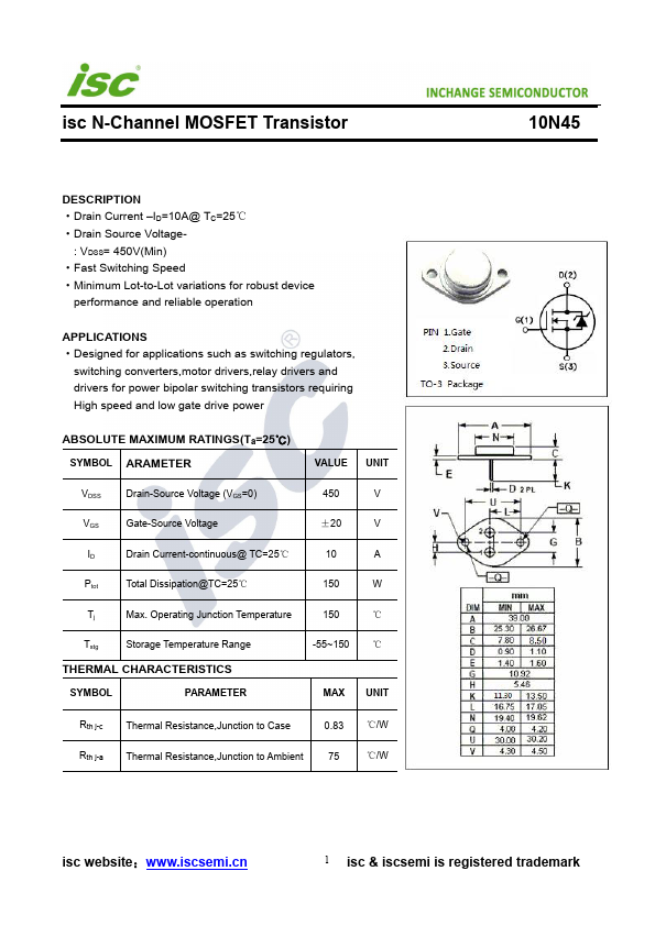
DESCRIPTION ·Drain Current –ID=10A@ TC=25℃ ·Drain Source Voltage-
: VDSS= 450V(Min) ·Fa...
isc N-Channel
MOSFET Transistor
DESCRIPTION ·Drain Current –ID=10A@ TC=25℃ ·Drain Source
Voltage-
: VDSS= 450V(Min) ·Fast Switching Speed ·Minimum Lot-to-Lot variations for robust device
performance and reliable operation
APPLICATIONS ·Designed for applications such as switching regulators,
switching converters,motor drivers,relay drivers and drivers for power bipolar switching transistors requiring High speed and low gate drive power
ABSOLUTE MAXIMUM RATINGS(Ta=25℃) SYMBOL ARAMETER
VALUE UNIT
VDSS
Drain-Source
Voltage (VGS=0)
450
V
VGS
Gate-Source
Voltage
±20
V
ID
Drain Current-continuous@ TC=25℃
10
A
Ptot
Total Dissipation@TC=25℃
150
W
Tj
Max. Operating Junction Temperature
150
℃
Tstg
Storage Temperature Range
THERMAL CHARACTERISTICS
SYMBOL
PARAMETER
-55~150 ℃ MAX UNIT
Rth j-c Thermal Resistance,Junction to Case
0.83 ℃/W
Rth j-a Thermal Resistance,Junction to Ambient
75
℃/W
10N45
isc website:www.iscsemi.cn
1 isc & iscsemi is registered trademark
isc N-Channel
Mosfet Transistor
·ELECTRICAL CHARACTERISTICS (TC=25℃)
SYMBOL
PARAMETER
CONDITIONS
V(BR)DSS Drain-Source Breakdown
Voltage
VGS= 0; ID= 0.25mA
VGS(th) Gate Threshold
Voltage
VDS= VGS; ID=0.25mA
RDS(on) Drain-Source On-stage Resistance VGS=10V; ID= 10A
IGSS
Gate Source Leakage Current
VGS= ±20V;VDS= 0
IDSS
Zero Gate
Voltage Drain Current
VDS=450V; VGS= 0
VSD
Forward On-
Voltage
IS= 10A; VGS=0
CISS
Input capacitance
COSS
Output capacitance
VDS=25V;
CRSS
Revers...