M29F200BT M29F200BB
2 Mbit (256Kb x8 or 128Kb x16, Boot Block) Single Supply Flash Memory
PRELIMINARY DATA
s SINGLE 5V±...
M29F200BT M29F200BB
2 Mbit (256Kb x8 or 128Kb x16, Boot Block) Single Supply Flash Memory
PRELIMINARY DATA
s SINGLE 5V±10% SUPPLY
VOLTAGE for PROGRAM, ERASE and READ OPERATIONS
s ACCESS TIME: 45ns s PROGRAMMING TIME
– 8µs per Byte/Word typical s 7 MEMORY BLOCKS
– 1 Boot Block (Top or Bottom Location) – 2 Parameter and 4 Main Blocks s PROGRAM/ERASE CONTROLLER – Embedded Byte/Word Program algorithm – Embedded Multi-Block/Chip Erase algorithm – Status Register Polling and Toggle Bits – Ready/Busy Output Pin s ERASE SUSPEND and RESUME MODES – Read and Program another Block during
Erase Suspend s UNLOCK BYPASS PROGRAM COMMAND
– Faster Production/Batch Programming s TEMPORARY BLOCK UNPROTECTION
MODE s LOW POWER CONSUMPTION
– Standby and Automatic Standby s 100,000 PROGRAM/ERASE CYCLES per
BLOCK s 20 YEARS DATA RETENTION
– Defectivity below 1 ppm/year s ELECTRONIC SIGNATURE
– Manufacturer Code: 0020h – M29F200BT Device Code: 00D3h – M29F200BB Device Code: 00D4h
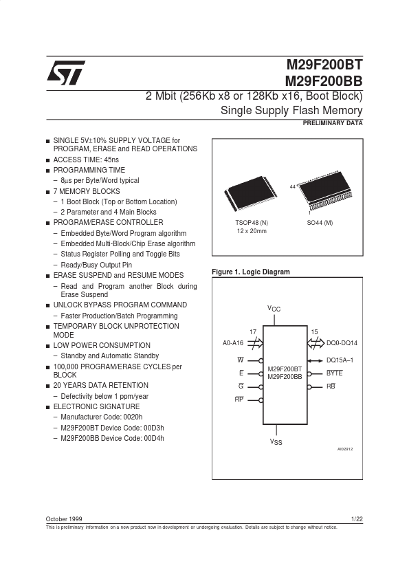
44
TSOP48 (N) 12 x 20mm
1
SO44 (M)
Figure 1. Logic Diagram
VCC
17 A0-A16
15 DQ0-DQ14
W DQ15A–1 M29F200BT
E M29F200BB BYTE G RB
RP
VSS
AI02912
October 1999
This is preliminary information on a new product now in development or undergoing evaluation. Details are subject to change without notice.
1/22
M29F200BT, M29F200BB
Figure 2A. TSOP Connections
A15 1
48 A16
A14 BYTE
A13 VSS A12 DQ15A–1
A11 DQ7
A10 DQ14
A9 DQ6
A8 DQ13
NC DQ5
NC DQ12
W DQ4
RP 12 M29F200BT 37 VCC NC 13 M29F200BB 36 DQ11
NC DQ3
RB D...