2N2905A 2N2907A
GENERAL PURPOSE AMPLIFIERS AND SWITCHES
DESCRIPTION The 2N2905A and 2N2907A are silicon planar epitaxial...
2N2905A 2N2907A
GENERAL PURPOSE
AMPLIFIERS AND SWITCHES
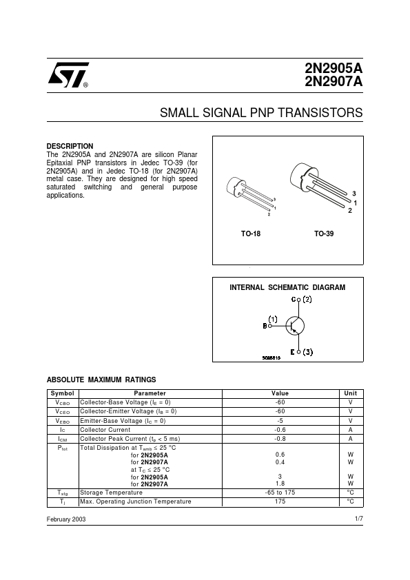
DESCRIPTION The 2N2905A and 2N2907A are silicon planar epitaxial PNP transistors in Jedec TO-39 (for 2N2905A) and in Jedec TO-18 (for 2N2907A) metal case. They are designed for high speed saturated switching and general purpose applications. 2N2905A approved to CECC 50002-100, 2N2906A approved to CECC 50002-103 available on request. TO-18 TO-39
INTERNAL SCHEMATIC DIAGRAM
ABSOLUTE MAXIMUM RATINGS
Symbol V CBO V CEO V EBO IC P t ot Parameter Collector-Base
Voltage (IE = 0) Collector-Emitter
Voltage (I B = 0) Emitter-Base
Voltage (I C = 0) Collector Current Total Dissipation at T amb ≤ 25 C for 2N2905A for 2N2907A at T case ≤ 25 o C for 2N2905A for 2N2907A St orage Temperature Max. Operating Junction Temperature
o
Value -60 -60 -5 -0.6 0.6 0.4 3 1.8 -65 to 200 200
Unit V V V A W W W W
o o
T stg Tj
C C 1/7
November 1997
2N2905A/2N2907A
THERMAL DATA
T O-39 R t hj-ca se R t hj- amb Thermal Resistance Junction-Case Thermal Resistance Junction-Ambient Max Max 58.3 292 TO -18 97.3 437.5
o o
C/W C/W
ELECTRICAL CHARACTERISTICS (Tcase = 25 oC unless otherwise specified)
Symb ol I CBO I CEX I BEX Parameter Collector Cut-off Current (IE = 0) Collector Cut-off Current (V BE = -0.5V) Base Cut-off Current (V BE = -0.5V) Test Cond ition s V CB = -50 V V CB = -50 V V CE = -30 V V CE = -30 V I C = -10 µ A -60 Tc ase = 150 C
o
Min.
Typ .
Max. -10 -10 -50 -50
Un it nA µA nA nA V
V ( BR)CBO ∗ Collector-Base Breakdown
Voltage (I ...