2N3019, 2N3019S, 2N3700
Low Power Transistors
NPN Silicon
Features
• MIL−PRF−19500/391 Qualified • Available as JAN, JAN...
2N3019, 2N3019S, 2N3700
Low Power Transistors
NPN Silicon
Features
MIL−PRF−19500/391 Qualified Available as JAN, JANTX, and JANTXV
MAXIMUM RATINGS (TA = 25°C unless otherwise noted)
Characteristic
Symbol Value
Collector −Emitter
Voltage
VCEO
80
Collector −Base
Voltage
VCBO
140
Emitter −Base
Voltage
VEBO
7.0
Collector Current − Continuous
IC 1.0
Total Device Dissipation @ TA = 25°C 2N3019, 2N3019S 2N3700
PT
800 500
Unit Vdc Vdc Vdc Adc mW
Total Device Dissipation @ TC = 25°C 2N3019, 2N3019S 2N3700
PT
W 5.0 1.0
Operating and Storage Junction Temperature Range
TJ, Tstg
−65 to +200
°C
THERMAL CHARACTERISTICS
Characteristic
Symbol Max
Unit
Thermal Resistance, Junction to Ambient 2N3019, 2N3019S 2N3700
RqJA
°C/W 195 325
Thermal Resistance, Junction to Case 2N3019, 2N3019S 2N3700
RqJC
°C/W 30 150
Stresses exceeding Maximum Ratings may damage the device. Maximum Ratings are stress ratings only. Functional operation above the Recommended Operating Conditions is not implied. Extended exposure to stresses above the Recommended Operating Conditions may affect device reliability.
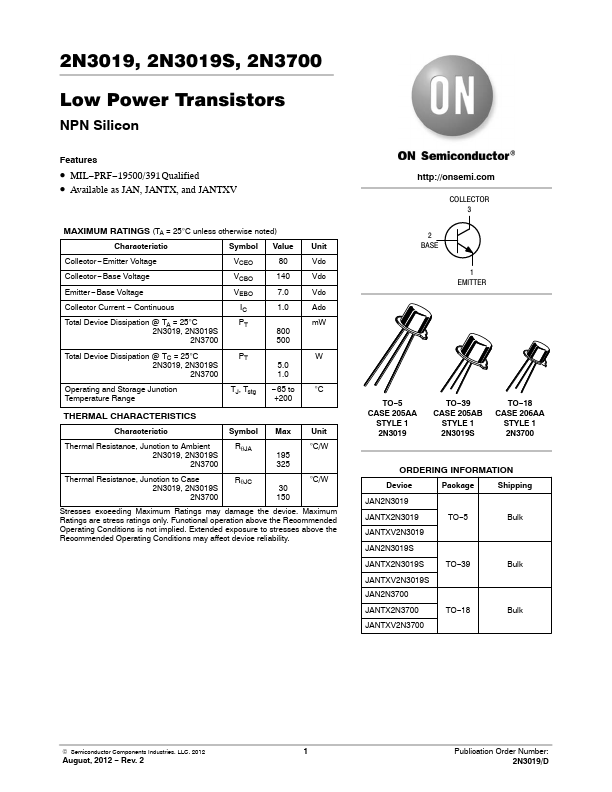
http://onsemi.com
COLLECTOR 3
2 BASE
1 EMITTER
TO−5 CASE 205AA
STYLE 1 2N3019
TO−39 CASE 205AB
STYLE 1 2N3019S
TO−18 CASE 206AA
STYLE 1 2N3700
ORDERING INFORMATION
Device
Package
Shipping
JAN2N3019
JANTX2N3019
TO−5
Bulk
JANTXV2N3019
JAN2N3019S
JANTX2N3019S
TO−39
Bulk
JANTXV2N3019S JAN2N3700
JANTX2N3700
TO−18
Bulk
JANTXV2N3700
© Semiconductor Component...