monolithic dual n-channel JFETs designed for • • •
• DiHerential Amplifiers
H
Siliconix
Performance Curves NNR See Sect...
monolithic dual n-channel JFETs designed for
DiHerential
Amplifiers
H
Siliconix
Performance Curves NNR See Section 4
BENEFITS
Minimum System Error and Calibration 5 mV Offset Maximum (2N3921)
Simplifies Amplifier Design Low Output Conductance
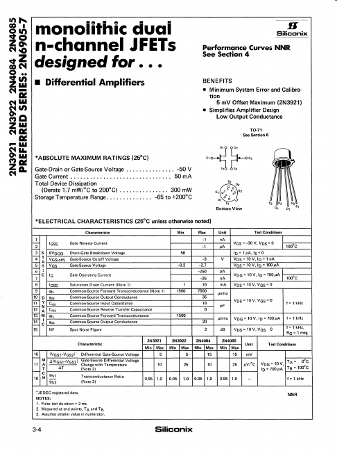
TO-71 See Section 6
*ABSOLUTE MAXIMUM RATINGS (25°C)
Gate-Drain or Gate-Source
Voltage .............. -50 V Gate Current ............................... 50 rnA Total Device Dissipation
(Derate 1.7 mW;oC to 200°C) .............. 300mW Storage Temperature Range ............. -65 to +200°C
~~G1 G2 81 S2
o'2 02
.,5 0
G, 0 3 6 0 27
0, 00'
G2
Bottom View
l~G.0, '
*ELECTRICAL CHARACTERISTICS (25°C unless otherwise noted)
Characteristic
.2. ~2 s
4"T -::-A
~:
-"b -c ...l...
8
IGSS
BVOGO VGS(offl VGS
IG
lOSS
9 9fs
100 gos
12":l1 V CISS Crss
13M 9fs
1_4c1 gos
15 NF
Gate Reverse Current
Drain-Gate Breakdown
Voltage Gate-Source Cutoff
Voltage Gate-5ource
Voltage
Gate Operatmg Current
Saturation Drain Current (Note 1) Common-Source Forward Transconductance (Note 1) Common-Source Output Conductance Common-Source Input Capacitance Common-Source Reverse Transfer Capacitance Common-Source Forward Transconductance Common-Source Output Conductance Spot NOise Figure
Min
50 -0.2
1 1500
1500
Max -1 -1
-3 -2.7 -250 -25
10 7500
35 18
6
20 2
Unit Test Conditions
nA
IVGS=-30V. VOS=O
IlA
100·C
10 = lilA. IS = 0
V VOS-l0V.10-lnA
VOS - 10V,I0 = lOOIlA
pA VOG = 10V,I0 = 700ilA
nA 100·C
mA VOS = 10V, VGS = 0
"mho pF
VOS=1...