2N5400, 2N5401
Preferred Device
Amplifier Transistors
PNP Silicon
Features
• Pb−Free Packages are Available*
http://o...
2N5400, 2N5401
Preferred Device
Amplifier Transistors
PNP Silicon
Features
Pb−Free Packages are Available*
http://onsemi.com
COLLECTOR 3
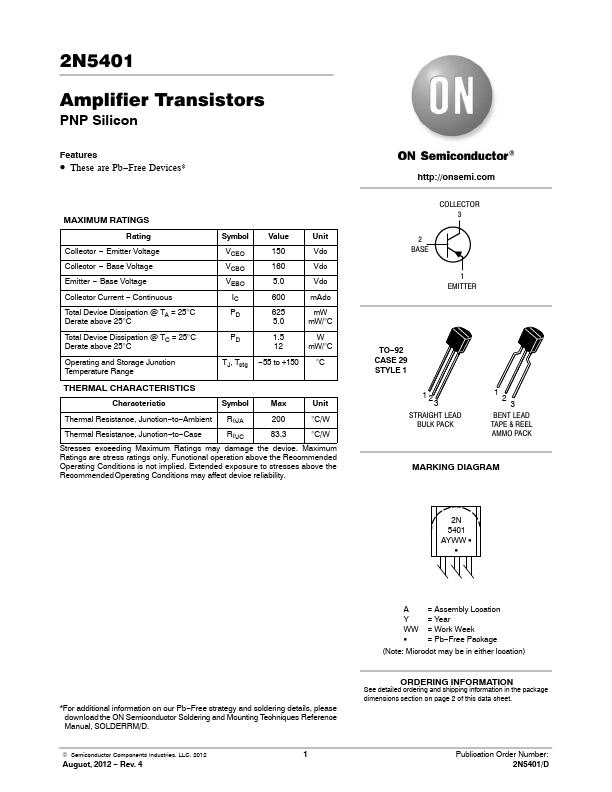
MAXIMUM RATINGS
Rating Collector − Emitter
Voltage Collector − Base
Voltage Emitter − Base
Voltage Collector Current − Continuous Total Device Dissipation @ TA = 25°C Derate above 25°C Total Device Dissipation @ TC = 25°C Derate above 25°C Operating and Storage Junction Temperature Range Symbol VCEO VCBO VEBO IC PD 625 5.0 PD 1.5 12 TJ, Tstg −55 to +150 Watts mW/°C °C 12 3 mW mW/°C TO−92 CASE 29 STYLE 1 2N5400 2N5401 120 130 5.0 600 150 160 Unit Vdc Vdc Vdc mAdc 1 EMITTER 2 BASE
Maximum ratings are those values beyond which device damage can occur. Maximum ratings applied to the device are individual stress limit values (not normal operating conditions) and are not valid simultaneously. If these limits are exceeded, device functional operation is not implied, damage may occur and reliability may be affected.
MARKING DIAGRAM
2N 540x AYWWG G
THERMAL CHARACTERISTICS
Characteristic Thermal Resistance, Junction−to−Ambient Thermal Resistance, Junction−to−Case Symbol RqJA RqJC Max 200 83.3 Unit °C/W °C/W
A = Assembly Location Y = Year WW = Work Week G = Pb−Free Package (Note: Microdot may be in either location)
ORDERING INFORMATION
See detailed ordering and shipping information in the package dimensions section on page 5 of this data sheet.
*For additional information on our Pb−Free strategy and soldering details, please download the ON...