www.DataSheet4U.com
2N5457, 2N5458
Preferred Device
JFETs − General Purpose
N−Channel − Depletion
N−Channel Junction F...
www.DataSheet4U.com
2N5457, 2N5458
Preferred Device
JFETs − General Purpose
N−Channel − Depletion
N−Channel Junction Field Effect Transistors, depletion mode (Type A) designed for audio and switching applications.
Features http://onsemi.com
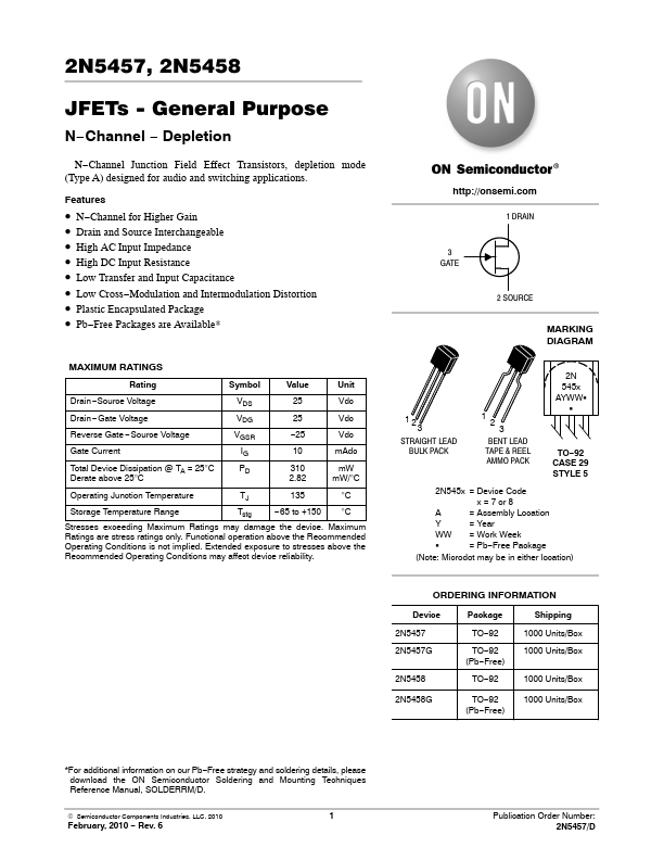
1 DRAIN
N−Channel for Higher Gain Drain and Source Interchangeable High AC Input Impedance High DC Input Resistance Low Transfer and Input Capacitance Low Cross−Modulation and Intermodulation Distortion Unibloc Plastic Encapsulated Package Pb−Free Packages are Available*
3 GATE
2 SOURCE
MARKING DIAGRAM
MAXIMUM RATINGS
Rating Drain −Source
Voltage Drain −Gate
Voltage Reverse Gate −Source
Voltage Gate Current Total Device Dissipation @ TA = 25°C Derate above 25°C Operating Junction Temperature Storage Temperature Range Symbol VDS VDG VGSR IG PD TJ Tstg Value 25 25 −25 10 310 2.82 135 −65 to +150 Unit Vdc Vdc Vdc mAdc mW mW/°C °C °C 12 3 TO−92 CASE 29 STYLE 5 2N 545x AYWWG G
Stresses exceeding Maximum Ratings may damage the device. Maximum Ratings are stress ratings only. Functional operation above the Recommended Operating Conditions is not implied. Extended exposure to stresses above the Recommended Operating Conditions may affect device reliability.
2N545x = Device Code x = 7 or 8 A = Assembly Location Y = Year WW = Work Week G = Pb−Free Package (Note: Microdot may be in either location)
ORDERING INFORMATION
Device 2N5457 2N5457G 2N5458 2N5458G Package TO−92 TO−92 (Pb−Free) TO−92 TO−92 (Pb−Free) Shipping 1000 Uni...