MOTOROLA
SEMICONDUCTOR TECHNICAL DATA
Order this document by 2N7002LT1/D
TMOS FET Transistor
N–Channel Enhancement
3 ...
MOTOROLA
SEMICONDUCTOR TECHNICAL DATA
Order this document by 2N7002LT1/D
TMOS FET Transistor
N–Channel Enhancement
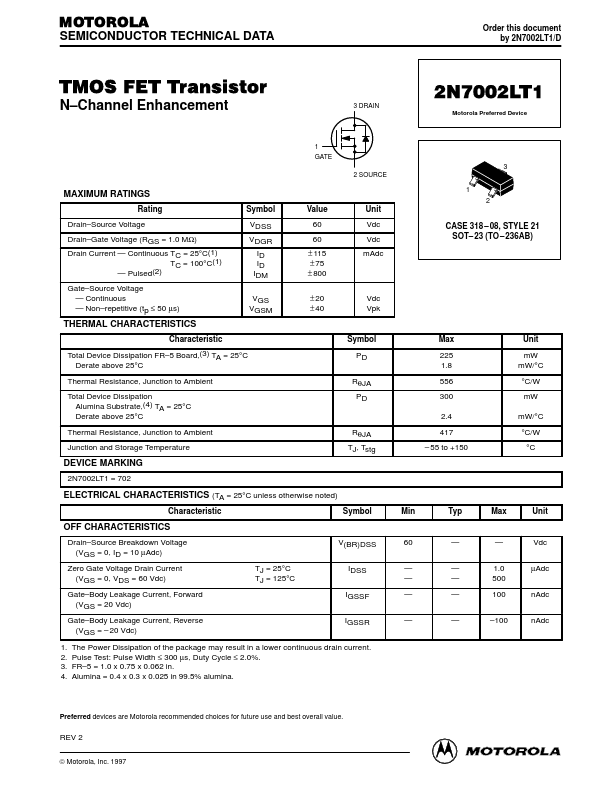
3 DRAIN 1 GATE
2N7002LT1
Motorola Preferred Device
3
2 SOURCE
MAXIMUM RATINGS
Rating Drain–Source
Voltage Drain–Gate
Voltage (RGS = 1.0 MΩ) Drain Current — Continuous TC = 25°C(1) Drain Current — Continuous TC = 100°C(1) Drain Current — Pulsed(2) Gate–Source
Voltage — Continuous — Non–repetitive (tp ≤ 50 µs) Symbol VDSS VDGR ID ID IDM VGS VGSM Value 60 60 ± 115 ± 75 ± 800 ± 20 ± 40 Unit Vdc Vdc mAdc
1 2
CASE 318 – 08, STYLE 21 SOT– 23 (TO – 236AB)
Vdc Vpk
THERMAL CHARACTERISTICS
Characteristic Total Device Dissipation FR–5 Board,(3) TA = 25°C Derate above 25°C Thermal Resistance, Junction to Ambient Total Device Dissipation Alumina Substrate,(4) TA = 25°C Derate above 25°C Thermal Resistance, Junction to Ambient Junction and Storage Temperature Symbol PD RθJA PD Max 225 1.8 556 300 2.4 RθJA TJ, Tstg 417 – 55 to +150 Unit mW mW/°C °C/W mW mW/°C °C/W °C
DEVICE MARKING
2N7002LT1 = 702
ELECTRICAL CHARACTERISTICS (TA = 25°C unless otherwise noted)
Characteristic Symbol Min Typ Max Unit
OFF CHARACTERISTICS
Drain–Source Breakdown
Voltage (VGS = 0, ID = 10 µAdc) Zero Gate
Voltage Drain Current (VGS = 0, VDS = 60 Vdc) Gate–Body Leakage Current, Forward (VGS = 20 Vdc) Gate–Body Leakage Current, Reverse (VGS = – 20 Vdc) 1. 2. 3. 4. TJ = 25°C TJ = 125°C V(BR)DSS IDSS IGSSF IGSSR 60 — — — — — — — — — — 1.0 500 100 –100 Vdc µAdc nAdc nAdc
The Power Dissipation o...