2SD974
Silicon NPN Epitaxial
Application
• Power switching • TV horizontal deflection output
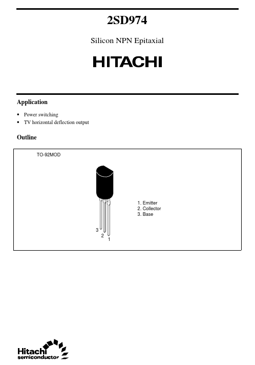
Outline
TO-92MOD
1. Emit...
2SD974
Silicon NPN Epitaxial
Application
Power switching TV horizontal deflection output
Outline
TO-92MOD
1. Emitter 2. Collector 3. Base 3 2 1
2SD974
Absolute Maximum Ratings (Ta = 25°C)
Item Collector to base
voltage Collector to emitter
voltage Emitter to base
voltage Collector current Collector peak current Surge collector current Collector power dissipation Junction temperature Storage temperature Symbol VCBO VCEO VEBO IC iC(peak) I C(surge) PC Tj Tstg Ratings 120 60 5 1 1.5 4 0.9 150 –55 to +150 Unit V V V A A A W °C °C
Electrical Characteristics (Ta = 25°C)
Item Collector to base breakdown
voltage Symbol V(BR)CBO Min 120 60 5 — 150 — — — Typ — — — — — — — 0.4 Max — — — 1.0 — 0.3 1.2 — V MHz pF I CP = 1 A, IB1 = –IB2 = 50 mA*1 Unit V V V µA Test conditions I C = 10 µA, IE = 0 I C = 1 mA, RBE = ∞ I E = 10 µA, IC = 0 VCB = 100 V, IE = 0 VCE = 5 V, IC = 1 A*1 I C = 1 A, IB = 0.05 A*1
Collector to emitter breakdown V(BR)CEO
voltage Emitter to base breakdown
voltage Collector cutoff current DC current transfer ratio Collector to emitter saturation
voltage Base to emitter saturation
voltage Fall time Note: 1. Pulse test V(BR)EBO I CBO hFE VCE(sat) VBE(sat) tf
2
2SD974
Maximum Collector Dissipation Curve 1.2 Collector Power Dissipation PC (W) Collector Current IC (A) Area of Safe Operaton 6 5 4 3 2 1 (20 V, 4 A) f = 15.75 kHz Ta = 25°C
0.8
0.4
(60 V, 0.5 A) 50 100 150 Collector to Emitter
Voltage VCE (V)
0
50 100 150 Ambient Temperature Ta (°C)
0
Typical Out...