DATA SHEET
MOS FIELD EFFECT TRANSISTOR
2SJ648
P-CHANNEL MOS FIELD EFFECT TRANSISTOR FOR SWITCHING
DESCRIPTION
The 2SJ...
DATA SHEET
MOS FIELD EFFECT TRANSISTOR
2SJ648
P-CHANNEL MOS FIELD EFFECT TRANSISTOR FOR SWITCHING
DESCRIPTION
The 2SJ648 is a switching device which can be driven directly by a 2.5 V power source. The 2SJ648 features a low on-state resistance and excellent switching characteristics, and is suitable for applications such as power switch of portable machine and so on.
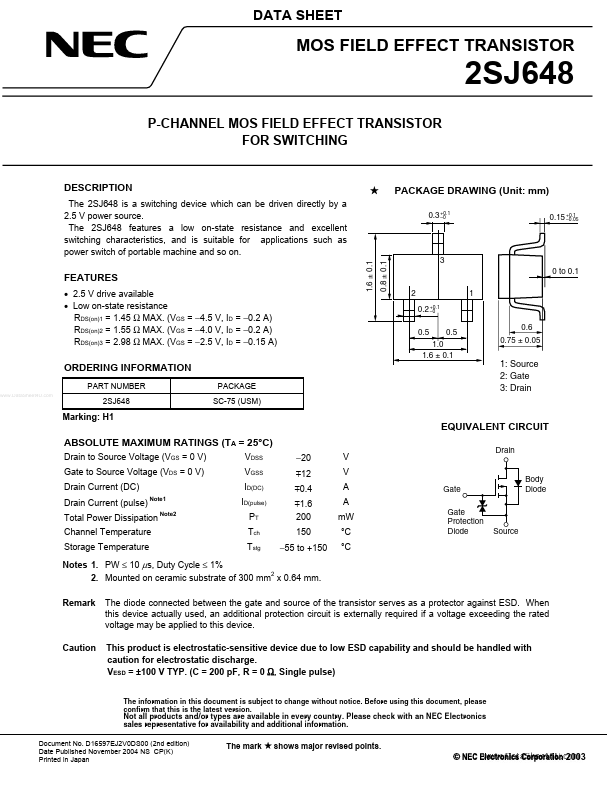
1.6 ± 0.1 0.8 ± 0.1
PACKAGE DRAWING (Unit: mm)
0.3 +0.1 –0 0.15 +0.1 –0.05
3 0 to 0.1 2 0.2 0.5
+0.1 –0
FEATURES
2.5 V drive available Low on-state resistance RDS(on)1 = 1.45 Ω MAX. (VGS = −4.5 V, ID = −0.2 A) RDS(on)2 = 1.55 Ω MAX. (VGS = −4.0 V, ID = −0.2 A) RDS(on)3 = 2.98 Ω MAX. (VGS = −2.5 V, ID = −0.15 A)
1
0.5
0.6 0.75 ± 0.05
1.0 1.6 ± 0.1
ORDERING INFORMATION
PART NUMBER
www.DataSheet4U.com
PACKAGE SC-75 (USM)
1: Source 2: Gate 3: Drain
2SJ648
Marking: H1
EQUIVALENT CIRCUIT
VDSS VGSS ID(DC) ID(pulse) PT Tch Tstg
Note2
ABSOLUTE MAXIMUM RATINGS (TA = 25°C)
Drain to Source
Voltage (VGS = 0 V) Gate to Source
Voltage (VDS = 0 V) Drain Current (DC) Drain Current (pulse) Note1 Total Power Dissipation Channel Temperature Storage Temperature −20 m12 m0.4 m1.6 200 150 −55 to +150 V V A A mW °C °C
Gate Protection Diode Gate
Drain
Body Diode
Source
Notes 1. PW ≤ 10 µs, Duty Cycle ≤ 1% 2 2. Mounted on ceramic substrate of 300 mm x 0.64 mm. Remark The diode connected between the gate and source of the transistor serves as a protector against ESD. When this device actually used, an additional pro...