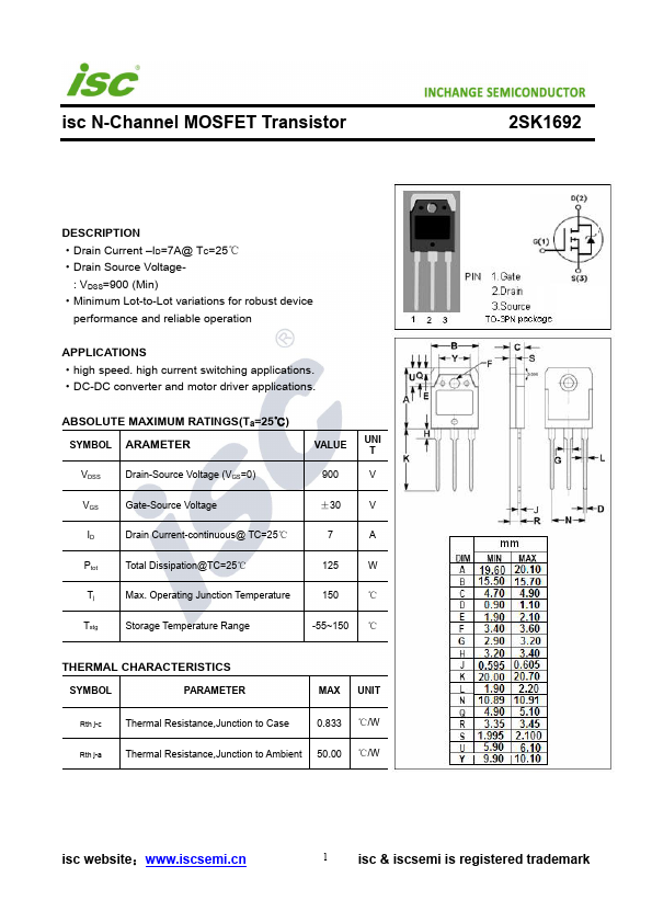
isc N-Channel MOSFET Transistor
2SK1692
DESCRIPTION ·Drain Current –ID=7A@ TC=25℃ ·Drain Source Voltage-
: VDSS=900 (M...
isc N-Channel
MOSFET Transistor
2SK1692
DESCRIPTION ·Drain Current –ID=7A@ TC=25℃ ·Drain Source
Voltage-
: VDSS=900 (Min) ·Minimum Lot-to-Lot variations for robust device
performance and reliable operation
APPLICATIONS ·high speed. high current switching applications. ·DC-DC converter and motor driver applications.
ABSOLUTE MAXIMUM RATINGS(Ta=25℃) SYMBOL ARAMETER
VDSS
Drain-Source
Voltage (VGS=0)
VALUE
UNI T
900
V
VGS
Gate-Source
Voltage
±30
V
ID
Drain Current-continuous@ TC=25℃
7
A
Ptot
Total Dissipation@TC=25℃
125
W
Tj
Max. Operating Junction Temperature
150
℃
Tstg
Storage Temperature Range
-55~150 ℃
THERMAL CHARACTERISTICS
SYMBOL
PARAMETER
MAX UNIT
Rth j-c Thermal Resistance,Junction to Case
0.833 ℃/W
Rth j-a
Thermal Resistance,Junction to Ambient 50.00 ℃/W
isc website:www.iscsemi.cn
1 isc & iscsemi is registered trademark
isc N-Channel
Mosfet Transistor
2SK1692
·ELECTRICAL CHARACTERISTICS (TC=25℃)
SYMBOL
PARAMETER
CONDITIONS
V(BR)DSS Drain-Source Breakdown
Voltage VGS=0; ID= 10mA
MIN TYP MAX UNIT
900
V
VGS(th) Gate Threshold
Voltage
VDS=10V; ID=1mA
RDS(on) Drain-Source On-stage Resistance VGS=10V; ID=3.5A
IGSS
Gate Source Leakage Current
VGS= ±25V;VDS= 0
IDSS
Zero Gate
Voltage Drain Current
VDS=720V; VGS= 0
1.5
3.5
V
1.7
2.0
Ω
±100 nA
300
uA
VSD
Diode Forward
Voltage
IF=7A; VGS=0
2.0
V
tr
Rise time
70
ns
ton
Turn-on time
tf
Fall time
100
ns
VGS=10V;ID=3.5A;RL=110Ω
100
ns
toff
Turn-off t...