o c . U 4 Features t e High speed switching e h Low on-resistance S No secondary breakdown apower t Low driving a High D...
o c . U 4 Features t e High speed switching e h Low on-resistance S No secondary breakdown apower t Low driving a High D
voltage . V =±35V Guarantee w Avalanche-proof w w
GS
2SK2642-01MR m
FUJI POWER MOS-FET
N-CHANNEL SILICON POWER MOS-FET
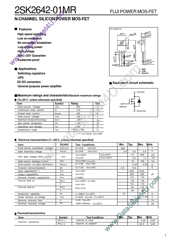
TO-220F15
2.54
Applications
Switching regulators UPS DC-DC converters General purpose power amplifier
Maximum ratings and characteristicAbsolute maximum ratings
(Tc=25°C unless otherwise specified)
Item Drain-source
voltage Continuous drain current Pulsed drain current Gate-source
voltage Maximum Avalanche Energy Max. power dissipation Operating and storage temperature range Symbol V DS ID ID(puls] VGS EAV *1 PD Tch Tstg Rating 500 ±15 ±60 ±35 88.7 50 +150 -55 to +150 Unit V A A V mJ W °C °C
Electrical characteristics (Tc =25°C unless otherwise specified)
Item Drain-source breakdown
voltaget Gate threshold
voltage Zero gate
voltage drain current Symbol V(BR)DSS VGS(th) IDSS
Gate-source leakage current Drain-source on-state resistance Forward transcondutance Input capacitance Output capacitance Reverse transfer capacitance Turn-on time ton Turn-off time toff Avalanche capability Diode forward on-
voltage Reverse recovery time Reverse recovery charge
m o .c U 4 t e e h S a t a .D w w w
Gate(G)
3. Source
Equivalent circuit schematic
Drain(D)
Source(S)
*1 L=0.72mH, Vcc=50V
Test Conditions ID=1mA VGS=0V ID=1mA VDS=VGS
Min.
Typ.
Max. Units
V V µA mA nA Ω S pF
500 3.5
IGSS RDS(on) gfs Ciss Coss Crss td(on) tr td(off) tf IAV V SD...