www.DataSheet4U.com
DATA SHEET
JUNCTION FIELD EFFECT TRANSISTOR
2SK3230
N-CHANNEL SILICON JUNCTION FIELD EFFECT TRANS...
www.DataSheet4U.com
DATA SHEET
JUNCTION FIELD EFFECT TRANSISTOR
2SK3230
N-CHANNEL SILICON JUNCTION FIELD EFFECT TRANSISTOR FOR IMPEDANCE CONVERTER OF ECM
DESCRIPTION
The 2SK3230 is suitable for converter of ECM.
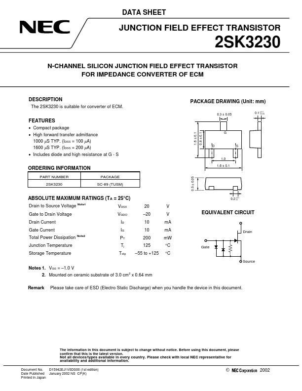
PACKAGE DRAWING (Unit: mm)
0.3 ± 0.05 0.1 +0.1 –0.05
FEATURES
Compact package High forward transfer admittance 1000 µS TYP. (IDSS = 100 µA) 1600 µS TYP. (IDSS = 200 µA) Includes diode and high resistance at G - S
1.0
1.6 ± 0.1 0.8 ± 0.1
G
D
S
ORDERING INFORMATION
2SK3230 SC-89 (TUSM)
0.5 ± 0.05
1.6 ± 0.1
PART NUMBER
PACKAGE
ABSOLUTE MAXIMUM RATINGS (TA = 25°C)
Drain to Source
Voltage Gate to Drain
Voltage Drain Current Gate Current Total Power Dissipation Junction Temperature Storage Temperature Notes 1. VGS = –1.0 V 2. Mounted on ceramic substrate of 3.0 cm x 0.64 mm Remark
2 Note2 Note1
0.2 +0.1 –0
VDSX VGDO ID IG PT Tj Tstg
20 –20 10 10 200 125 –55 to +125
V V mA mA mW °C °C
Source Gate Drain
EQUIVALENT CIRCUIT
Please take care of ESD (Electro Static Discharge) when you handle the device in this document.
The information in this document is subject to change without notice. Before using this document, please confirm that this is the latest version.
Not all devices/types available in every country. Please check with local NEC representative for availability and additional information.
Document No. D15942EJ1V0DS00 (1st edition) Date Published January 2002 NS CP(K) Printed in Japan
©
2002
2SK3230
ELECTRICAL CHARACTERISTICS (TA = 25°C)
CH...