DataSheet.in
TENTATIVE
TOSHIBA Field Effect Transistor Silicon N Channel MOS Type (π-MOSⅥ)
2SK3563
2SK3563
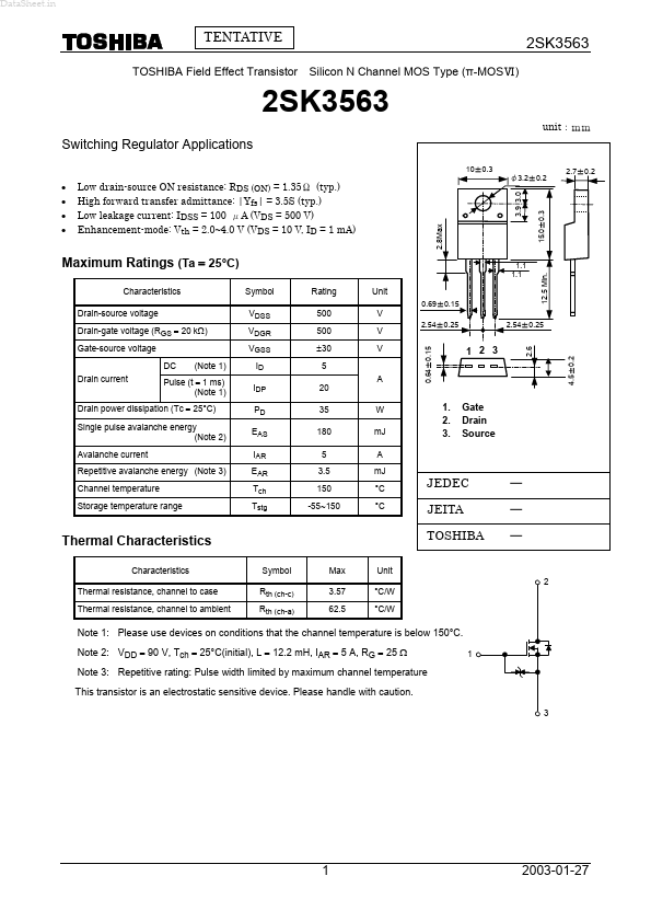
unit:mm
S...
DataSheet.in
TENTATIVE
TOSHIBA Field Effect Transistor Silicon N Channel MOS Type (π-MOSⅥ)
2SK3563
2SK3563
unit:mm
Switching Regulator Applications
10±0.3
Maximum Ratings (Ta = 25°C)
Characteristics Drain-source
voltage Drain-gate
voltage (RGS = 20 kΩ) Gate-source
voltage DC Drain current (Note 1) Symbol VDSS VDGR VGSS ID IDP PD EAS IAR EAR Tch Tstg Rating 500 500 ±30 5 20 35 180 5 3.5 150 -55~150 A W mJ A mJ °C °C Unit
0.69±0.15
2.8Max
V V V
2.54±0.25 0.64±0.15 2.54±0.25 2.6
Pulse (t = 1 ms) (Note 1)
Drain power dissipation (Tc = 25°C) Single pulse avalanche energy (Note 2) Avalanche current Repetitive avalanche energy (Note 3) Channel temperature Storage temperature range
1. 2. 3.
Gate Drain Source
JEDEC JEITA TOSHIBA
― ― ―
Thermal Characteristics
Characteristics Thermal resistance, channel to case Thermal resistance, channel to ambient Symbol Rth (ch-c) Rth (ch-a) Max 3.57 62.5 Unit
2 °C/W °C/W
Note 1: Please use devices on conditions that the channel temperature is below 150°C. Note 2: VDD = 90 V, Tch = 25°C(initial), L = 12.2 mH, IAR = 5 A, RG = 25 Ω Note 3: Repetitive rating: Pulse width limited by maximum channel temperature This transistor is an electrostatic sensitive device. Please handle with caution.
3 1
1
2003-01-27
4.5±0.2
1 2 3
12.5 Min.
1.1 1.1
15.0±0.3
Low drain-source ON resistance: RDS (ON) = 1.35Ω (typ.) High forward transfer admittance: |Yfs| = 3.5S (typ.) Low leakage current: IDSS = 100 μA (VDS = 500 V) Enhancement-mode: ...