isc N-Channel MOSFET Transistor
DESCRIPTION ·Drain Current –ID=8A@ TC=25℃ ·Drain Source Voltage-
: VDSS=200V(Min) ·Fast...
isc N-Channel
MOSFET Transistor
DESCRIPTION ·Drain Current –ID=8A@ TC=25℃ ·Drain Source
Voltage-
: VDSS=200V(Min) ·Fast Switching Speed ·100% avalanche tested ·Minimum Lot-to-Lot variations for robust device
performance and reliable operation
APPLICATIONS ·low on–resistance ·High speed switching ·Low drive current ·No secondary breakdown ·Suitable for switchingregulator, DC–DC convertor
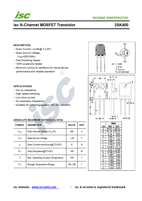
ABSOLUTE MAXIMUM RATINGS(Ta=25℃) SYMBOL ARAMETER
VALUE UNIT
VDSS
Drain-Source
Voltage (VGS=0)
200
V
VGS
Gate-Source
Voltage
±20
V
ID
Drain Current-continuous@ TC=25℃
8
A
Ptot
Total Dissipation@TC=25℃
100
W
Tj
Max. Operating Junction Temperature
150
℃
Tstg
Storage Temperature Range
-55~150 ℃
2SK400
isc website:www.iscsemi.com
1 isc & iscsemi is registered trademark
isc N-Channel
MOSFET Transistor
·ELECTRICAL CHARACTERISTICS (TC=25℃)
SYMBOL
PARAMETER
CONDITIONS
V(BR)DSS Drain-Source Breakdown
Voltage VGS=0; ID= 10mA
VGS(TH) Gate Threshold
Voltage
VDS= 10V; ID= 1mA
RDS(ON) Drain-Source On-stage Resistance VGS= 15V; ID=4A
VSD
Drain Forward
Voltage
IF=4A; VGS=0
IGSS
Gate Source Leakage Current
VGS= ±20V; VDS= 0
IDSS
Zero Gate
Voltage Drain Current
VDS=160V; VGS= 0
2SK400
MIN TYP. MAX UNIT
200
V
2.0
5.0
V
0.5
0.7
Ω
0.9
V
±1
uA
1
mA
NOTICE: ISC reserves the rights to make changes of the content herein the datasheet at any time without notification. The information contained herein is presented only as a guide for the applications of our...