DATA SHEET
www.DataSheet4U.com
JUNCTION FIELD EFFECT TRANSISTOR
2SK4028
N-CHANNEL SILICON JUNCTION FIELD EFFECT TRANS...
DATA SHEET
www.DataSheet4U.com
JUNCTION FIELD EFFECT TRANSISTOR
2SK4028
N-CHANNEL SILICON JUNCTION FIELD EFFECT TRANSISTOR FOR IMPEDANCE CONVERTER OF ECM
DESCRIPTION
The 2SK4028 is suitable for converter of ECM.
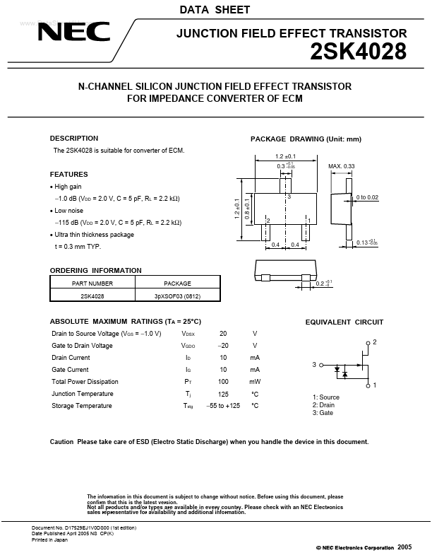
PACKAGE DRAWING (Unit: mm)
1.2 ±0.1 0.3 –0.05
+0.1
MAX. 0.33
FEATURES
High gain
1.2 ±0.1
Low noise −115 dB (VDD = 2.0 V, C = 5 pF, RL = 2.2 kΩ) Ultra thin thickness package t = 0.3 mm TYP.
0.8 ±0.1
−1.0 dB (VDD = 2.0 V, C = 5 pF, RL = 2.2 kΩ)
3
0 to 0.02
2
1
0.4
0.4
0.13 –0.05
+0.1
ORDERING INFORMATION
PART NUMBER 2SK4028 PACKAGE 3pXSOF03 (0812)
0.2 +0.1 –0
ABSOLUTE MAXIMUM RATINGS (TA = 25°C)
Drain to Source
Voltage (VGS = −1.0 V) Gate to Drain
Voltage Drain Current Gate Current Total Power Dissipation Junction Temperature Storage Temperature VDSX VGDO ID IG PT Tj Tstg 20 −20 10 10 100 125 −55 to +125 V V mA mA mW °C °C
EQUIVALENT CIRCUIT
2
3 1 1: Source 2: Drain 3: Gate
Caution Please take care of ESD (Electro Static Discharge) when you handle the device in this document.
The information in this document is subject to change without notice. Before using this document, please confirm that this is the latest version.
Not all products and/or types are available in every country. Please check with an NEC Electronics sales representative for availability and additional information.
Document No. D17529EJ1V0DS00 (1st edition) Date Published April 2005 NS CP(K) Printed in Japan
2005
2SK4028
ELECTRICAL CHARACTERISTICS (TA = 25°C)
CHARACTERIS...