54AC16543, 74AC16543 16ĆBIT REGISTERED TRANSCEIVERS
WITH 3ĆSTATE OUTPUTS
SCAS125B − MARCH 1990 − REVISED APRIL 1996
D M...
54AC16543, 74AC16543 16ĆBIT REGISTERED TRANSCEIVERS
WITH 3ĆSTATE OUTPUTS
SCAS125B − MARCH 1990 − REVISED APRIL 1996
D Members of the Texas Instruments
Widebus Family
D 3-State True Outputs
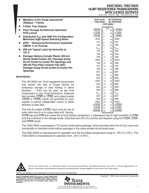
54AC16543 . . . WD PACKAGE 74AC16543 . . . DL PACKAGE
(TOP VIEW)
D Flow-Through Architecture Optimizes
1OEAB 1
56 1OEBA
PCB Layout
1LEAB 2
55 1LEBA
D Distributed VCC and GND Pin Configuration
Minimizes High-Speed Switching Noise
D EPIC (Enhanced-Performance Implanted
CMOS) 1-µm Process
D 500-mA Typical Latch-Up Immunity at
125°C
D Package Options Include Plastic 300-mil
Shrink Small-Outline (DL) Package Using 25-mil Center-to-Center Pin Spacings and 380-mil Fine-Pitch Ceramic Flat (WD) Package Using 25-mil Center-to-Center Pin Spacings
1CEAB GND 1A1 1A2 VCC 1A3 1A4 1A5 GND 1A6 1A7 1A8 2A1
3 4 5 6 7 8 9 10 11 12 13 14 15
54 1CEBA 53 GND 52 1B1 51 1B2 50 VCC 49 1B3 48 1B4 47 1B5 46 GND 45 1B6 44 1B7 43 1B8 42 2B1
description
2A2 16 2A3 17
41 2B2 40 2B3
The ’AC16543 are 16-bit registered transceivers that contain two sets of D-type latches for temporary storage of data flowing in either direction. They can be used as two 8-bit transceivers or one 16-bit transceiver. Separate latch-enable (LEAB or LEBA) and output-enable (OEAB or OEBA) inputs are provided for each
GND 2A4 2A5 2A6 VCC 2A7 2A8
18 19 20 21 22 23 24
39 GND 38 2B4 37 2B5 36 2B6 35 VCC 34 2B7 33 2B8
register to permit independent control in either
GND 25 32 GND
direction of data flow.
2CEAB 26 31 2CEBA
The...