Octal D Flip-Flop
www.DataSheet4U.com
54AC377 • 54ACT377 Octal D Flip-Flop with Clock Enable
February 1999
54AC377 • 54ACT377 Octal D F...
Description
www.DataSheet4U.com
54AC377 54ACT377 Octal D Flip-Flop with Clock Enable
February 1999
54AC377 54ACT377 Octal D Flip-Flop with Clock Enable
General Description
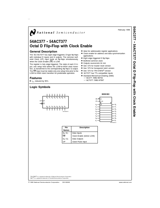
The ’AC/’ACT377 has eight edge-triggered, D-type flip-flops with individual D inputs and Q outputs. The common buffered Clock (CP) input loads all flip-flops simultaneously, when the Clock Enable (CE) is LOW. The register is fully edge-triggered. The state of each D input, one setup time before the LOW-to-HIGH clock transition, is transferred to the corresponding flip-flop’s Q output. The CE input must be stable only one setup time prior to the LOW-to-HIGH clock transition for predictable operation. n Ideal for addressable register applications n Clock enable for address and data synchronization applications n Eight edge-triggered D flip-flops n Buffered common clock n Outputs source/sink 24 mA n See ’273 for master reset version n See ’373 for transparent latch version n See ’374 for TRI-STATE ® version n ’ACT377 has TTL-compatible inputs n Standard Microcircuit Drawing (SMD) — ’AC377: 5962-88702 — ’ACT377: 5962-87697
Features
n ICC reduced by 50%
Logic Symbols
IEEE/IEC
DS100290-1
DS100290-2
Pin Names D0–D7 CE Q0–Q7 CP
Description Data Inputs Clock Enable (Active LOW) Data Outputs Clock Pulse Input
TRI-STATE ® is a registered trademark of National Semiconductor Corporation. FACT ® is a registered trademark of Fairchild Semiconductor Corporation.
© 1999 National Semiconductor Corporation
DS100290
www.n...
Similar Datasheet