www.DataSheet4U.com
54ACT112 Dual JK Negative Edge-Triggered Flip-Flop
September 1998
54ACT112 Dual JK Negative Edge-...
www.DataSheet4U.com
54ACT112 Dual JK Negative Edge-Triggered Flip-Flop
September 1998
54ACT112 Dual JK Negative Edge-Triggered Flip-Flop
General Description
The ’ACT112 contains two independent, high-speed JK flip-flops with Direct Set and Clear inputs. Synchronous state changes are initiated by the falling edge of the clock. Triggering occurs at a
voltage level of the clock and is not directly related to the transition time. The J and K inputs can change when the clock is in either state without affecting the flip-flop, provided that they are in the desired state during the recommended setup and hold times relative to the falling edge of the clock. A LOW signal on SD or CD prevents clocking and forces Q or Q HIGH, respectively. Simultaneous LOW signals on SD and CD force both Q and Q HIGH. Asynchronous Inputs: LOW input to SD sets Q to HIGH level LOW input to CD sets Q to LOW level Clear and Set are independent of clock Simultaneous LOW on CD and SD makes both Q and Q HIGH
Features
n ’ACT112 has TTL-compatible inputs n Outputs source/sink 24 mA n Standard Microcircuit Drawing (SMD) 5962-8995001
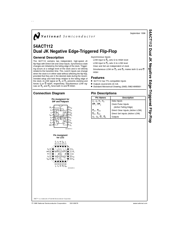
Connection Diagram
Pin Assigment for DIP and Flatpack
Pin Descriptions
Pin Names J1, J2, K1, K2 CP1, CP2 CD1, CD2 SD1, SD2 Q1, Q2, Q1, Q2 Data Inputs Clock Pulse Inputs (Active Falling Edge) Direct Clear Inputs (Active LOW) Direct Set Inputs (Active LOW) Outputs Description
DS100976-3
Pin Assigment for LCC
DS100976-5
FACT™ is a trademark of Fairchild Semiconductor Corporatio...