• Inputs Are TTL-Voltage Compatible • 3-State Outputs Drive Bus Lines or Buffer
Memory Address Registers
• Flow-Through ...
Inputs Are TTL-
Voltage Compatible 3-State Outputs Drive Bus Lines or Buffer
Memory Address Registers
Flow-Through Architecture to Optimize
PCB Layout
Center-Pin VCC and GND Configurations
Minimize High-Speed Switching Noise
t EPIC (Enhanced-Performance Implanted
CMOS) 1-mm Process
500-mA Typical Latch-Up Immunity
at 125°C
Package Options Include Plastic
Small-Outline Packages, Ceramic Chip
Carriers, and Standard Ceramic 300-mil
DIPs
description
These 10-bit buffers/bus drivers provide highperformance bus interface for wide data paths or buses carrying parity.
The 3-state control gate is a 2-input NOR such that if either G1 or G2 is high, all ten outputs are in the high-impedance state.
The ′ACT11827 provides inverted data.
The 54ACT11827 is characterized for operation over the full military temperature range of – 55°C to 125°C. The 74ACT11827 is characterized for operation from – 40°C to 85°C.
FUNCTION TABLE
INPUTS G1 G2 A
OUTPUT Y
L LH
H
LLL
L
XHX
Z
HXX
Z
Y5 GND GND GND GND
Y6 Y7
54ACT11827, 74ACT11827 10-BIT BUFFERS/BUS DRIVERS
WITH 3-STATE OUTPUTS
SCAS078 – NOVEMBER 1989 – REVISED APRIL 1993
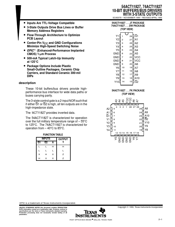
54ACT11827 . . . JT PACKAGE 74ACT11827 . . . DW PACKAGE
(TOP VIEW)
Y1 Y2 Y3 Y4 Y5 GND GND GND GND Y6 Y7 Y8 Y9 Y10
1 2 3 4 5 6 7 8 9 10 11 12 13 14
28 G1 27 A1 26 A2 25 A3 24 A4 23 A5 22 VCC 21 VCC 20 A6 19 A7 18 A8 17 A9 16 A10 15 G2
54ACT11827 . . . FK PACKAGE (TOP VIEW)
A3 A4 A5 VCC VCC A6 A7
4 3 2 1 28 27 26
A2 5
25 A8
A1 6
24 A9
G1 7
23 A10
Y...