Octal D Flip-Flop
54F 74F377 Octal D Flip-Flop with Clock Enable
Obsolete
May 1995
54F 74F377 Octal D Flip-Flop with Clock Enable
Gene...
Description
54F 74F377 Octal D Flip-Flop with Clock Enable
Obsolete
May 1995
54F 74F377 Octal D Flip-Flop with Clock Enable
General Description
The ’F377 has eight edge-triggered D-type flip-flops with individual D inputs and Q outputs The common buffered Clock (CP) input loads all flip-flops simultaneously when the Clock Enable (CE) is LOW
The register is fully edge-triggered The state of each D input one setup time before the LOW-to-HIGH clock transition is transferred to the corresponding flip-flop’s Q output The CE input must be stable only one setup time prior to the LOW-to-HIGH clock transition for predictable operation
Features
Y Ideal for addressable register applications Y Clock enable for address and data synchronization
applications Y Eight edge-triggered D flip-flops Y Buffered common clock Y See ’F273 for master reset version Y See ’F373 for transparent latch version Y See ’F374 for TRI-STATE version Y Guaranteed 4000V minimum ESD protection
Commercial 74F377PC
74F377SC (Note 1) 74F377SJ (Note 1)
Military 54F377DM (QB)
54F377FM (QB) 54F377LM (QB)
Package Number N20A J20A M20B M20D W20A E20A
Package Description
20-Lead (0 300 Wide) Molded Dual-In-Line 20-Lead Ceramic Dual-In-Line 20-Lead (0 300 Wide) Molded Small Outline JEDEC 20-Lead (0 300 Wide) Molded Small Outline EIAJ 20-Lead Cerpack 20-Lead Ceramic Leadless Chip Carrier Type C
Note 1 Devices also available in 13 reel Use suffix e SCX and SJX
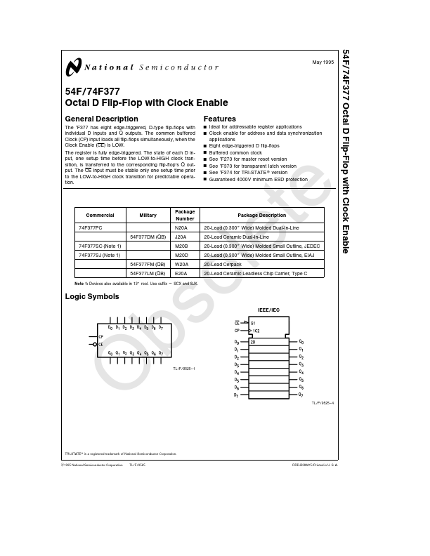
Logic Symbols
IEEE IEC
TL F 9525 – 1
TRI-STATE is a registered tra...
Similar Datasheet