55N03L
S eptember , 2002
N-Channel Logic Level E nhancement Mode Field E ffect Transistor
4 P R ODUC T S UMMAR Y
F E A...
55N03L
S eptember , 2002
N-Channel Logic Level E nhancement Mode Field E ffect Transistor
4 P R ODUC T S UMMAR Y
F E AT UR E S
VDS S 30V
ID R DS (on) ( m W ) T Y P
12.5 @ VGS = 10V 55A
20 @ VGS = 4.5V
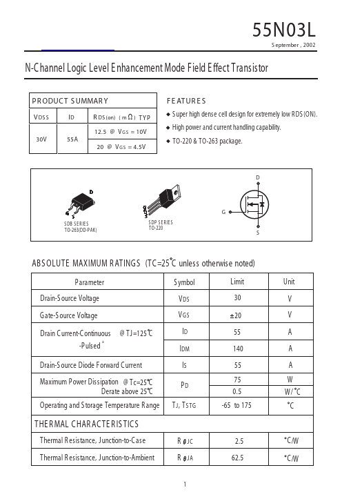
S uper high dense cell design for extremely low R DS (ON). High power and current handling capability. TO-220 & TO-263 package.
D
GS S DB S E R IE S T O -263(DD-P AK )
G D S
S DP S E R IE S TO-220
D
G S
ABS OLUTE MAXIMUM R ATINGS (TC =25 C unless otherwise noted)
P arameter Drain-S ource
Voltage Gate-S ource
Voltage
S ymbol VDS VGS
Limit 30 20
Drain C urrent-C ontinuous @ TJ=125 C -P ulsed a
ID IDM
55 140
Drain-S ource Diode Forward C urrent
Maximum P ower Dissipation @ Tc=25 C Derate above 25 C
Operating and S torage Temperature R ange
IS PD TJ, TSTG
55
75 0.5 -65 to 175
THE R MAL CHAR ACTE R IS TICS
Thermal R esistance, Junction-to-C ase
R JC
2.5
Thermal R esistance, Junction-to-Ambient
R JA
62.5
1
Unit V V A A A W W/ C C
C /W C /W
55N03L
E LE CTR ICAL CHAR ACTE R IS TICS (TC =25 C unless otherwise noted)
4 Parameter
S ymbol Condition
Min Typ Max Unit
OFF CHARACTERISTICS
Drain-S ource Breakdown
Voltage
Zero Gate
Voltage Drain Current Gate-Body Leakage
ON CHARACTERISTICS a
BVDSS VGS =0V, ID =250uA
30
IDSS VDS =24V, VGS =0V
IGSS VGS = 16V, VDS =0V
V 10 uA 100 nA
Gate Threshold
Voltage
VGS(th) VDS =VGS, ID = 250uA 1 1.5 3 V
Drain-S ource On-S tate R esistance
R DS(ON)
VGS = 10V, ID = 27A VGS = 4.5V, ID = 22A
12.5 14 m ohm 20 23 m ohm
O...