GT60N321
TOSHIBA Insulated Gate Bipolar Transistor Silicon N Channel IGBT
GT60N321
High-Power Switching Applications Fo...
GT60N321
TOSHIBA Insulated Gate Bipolar Transistor Silicon N Channel IGBT
GT60N321
High-Power Switching Applications Fourth Generation IGBT
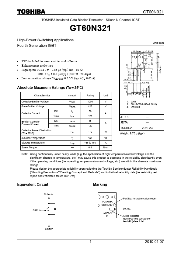
Unit: mm
FRD included between emitter and collector Enhancement mode type High speed IGBT : tf = 0.25 μs (typ.) (IC = 60 A)
FRD : trr = 0.8 μs (typ.) (di/dt = −20 A/μs) Low saturation
voltage: VCE (sat) = 2.3 V (typ.) (IC = 60 A)
Absolute Maximum Ratings (Ta = 25°C)
Characteristics
symbol
Rating
Unit
Collector-Emitter
Voltage
Gate-Emitter
Voltage
Collector Current
DC 1 ms
Emitter-Collector Forward Current
DC 1 ms
Collector Power Dissipation (Tc = 25°C)
Junction Temperature
Storage Temperature
Screw Torque
VCES VGES
IC ICP IECF IECFP
PC
Tj Tstg ⎯
1000 ±25 60 120 15 120
170
150 −55 to 150
0.8
V V A
A
W °C °C N・m
JEDEC
―
JEITA
―
TOSHIBA
2-21F2C
Weight: 9.75 g (typ.)
Note: Using continuously under heavy loads (e.g. the application of high temperature/current/
voltage and the significant change in temperature, etc.) may cause this product to decrease in the reliability significantly even if the operating conditions (i.e. operating temperature/current/
voltage, etc.) are within the absolute maximum ratings. Please design the appropriate reliability upon reviewing the Toshiba Semiconductor Reliability Handbook (“Handling Precautions”/“Derating Concept and Methods”) and individual reliability data (i.e. reliability test report and estimated failure rate, etc).
Equivalent Circuit
Marking
Collector Gate
Emitter...