FDS6986S
September 2002
FDS6986S
Dual Notebook Power Supply N-Channel PowerTrench SyncFET™
General Description
The FD...
FDS6986S
September 2002
FDS6986S
Dual Notebook Power Supply N-Channel PowerTrench SyncFET™
General Description
The FDS6986S is designed to replace two single SO-8
MOSFETs and Schottky diode in synchronous DC:DC power supplies that provide various peripheral
voltages for notebook computers and other battery powered electronic devices. FDS6986S contains two unique 30V, N-channel, logic level, PowerTrench
MOSFETs designed to maximize power conversion efficiency. The high-side switch (Q1) is designed with specific emphasis on reducing switching losses while the lowside switch (Q2) is optimized to reduce conduction losses. Q2 also includes an integrated Schottky diode using Fairchild’s monolithic SyncFET technology.
Features
Q2: Optimized to minimize conduction losses Includes SyncFET Schottky body diode RDS(on) = 20 mΩ @ VGS = 10V RDS(on) = 28 mΩ @ VGS = 4.5V Q1: Optimized for low switching losses Low gate charge (6.5 nC typical) RDS(on) = 29 mΩ @ VGS = 10V RDS(on) = 38 mΩ @ VGS = 4.5V
7.9A, 30V
6.5A, 30V
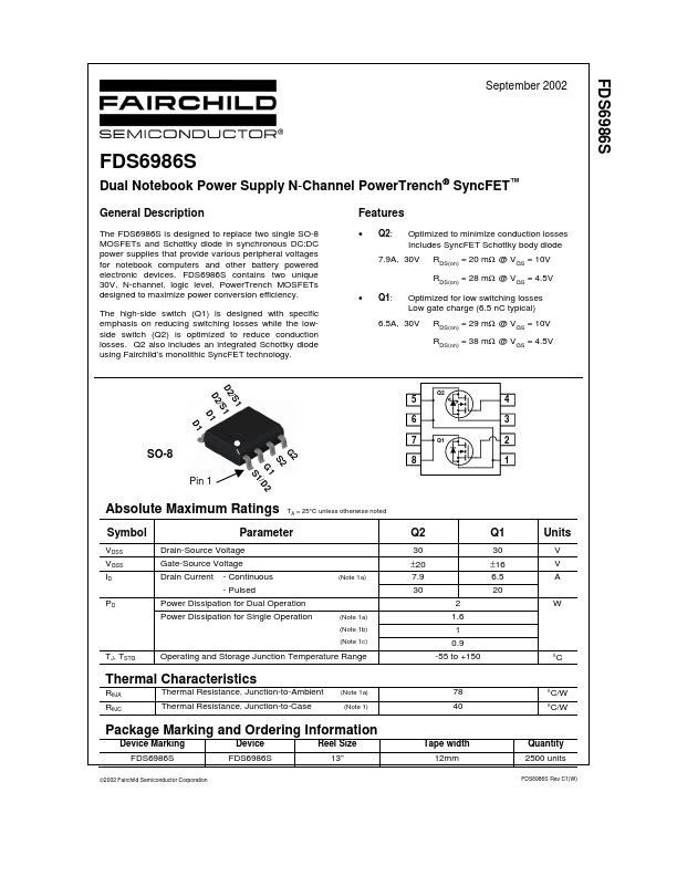
1 /S D2 1 /S D2
D
D
D
5 6 7
Q2
4 3
D1
D
D1
Q1
2 1
SO-8
G S1
Pin 1 SO-8
S
S
S
G S2 1 2 /D
http://www.DataSheet4U.net/
G
8
2
Absolute Maximum Ratings
Symbol
VDSS VGSS ID PD Drain-Source
Voltage Gate-Source
Voltage
TA = 25°C unless otherwise noted
Parameter
Q2
30
(Note 1a)
Q1
30 ±16 6.5 20 2 1.6 1 0.9 -55 to +150
Units
V V A W
- Continuous - Pulsed Power Dissipation for Dual Operation Power Dissipation for Single Operation
Drain Current
±20 ...