HIGH-SPEED 3.3V 128K x 36 SYNCHRONOUS BANK-SWITCHABLE DUAL-PORT STATIC RAM
HIGH-SPEED 3.3V 128K x 36 SYNCHRONOUS BANK-SWITCHABLE DUAL-PORT STATIC RAM WITH 3.3V OR 2.5V INTERFACE
70V7599S
Featur...
Description
HIGH-SPEED 3.3V 128K x 36 SYNCHRONOUS BANK-SWITCHABLE DUAL-PORT STATIC RAM WITH 3.3V OR 2.5V INTERFACE
70V7599S
Features:
◆ 128K x 36 Synchronous Bank-Switchable Dual-ported SRAM Architecture – 64 independent 2K x 36 banks – 4 megabits of memory on chip
◆ Bank access controlled via bank address pins ◆ High-speed data access
– Commercial: 3.4ns (200MHz)/3.6ns (166MHz)/ 4.2ns (133MHz) (max.)
◆ Selectable Pipelined or Flow-Through output mode ◆ Counter enable and repeat features ◆ Dual chip enables allow for depth expansion without
additional logic ◆ Supports JTAG features compliant with IEEE 1149.1
◆ Full synchronous operation on both ports – 5ns cycle time, 200MHz operation (14Gbps bandwidth) – Fast 3.4ns clock to data out – 1.5ns setup to clock and 0.5ns hold on all control, data, and address inputs @ 200MHz – Data input, address, byte enable and control registers – Self-timed write allows fast cycle time
◆ Separate byte controls for multiplexed bus and bus matching compatibility
◆ LVTTL- compatible, 3.3V (±150mV) power supply for core
◆ LVTTL compatible, selectable 3.3V (±150mV) or 2.5V (±100mV) power supply for I/Os and control signals on each port
◆ Available in a 208-pin fine pitch Ball Grid Array (fpBGA), and 256-pin Ball Grid Array (BGA)
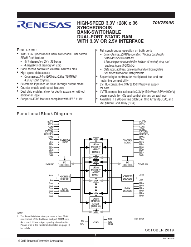
Functional Block Diagram
PL/FTL
OPTL
CLKL ADSL CNTENL REPEATL R/WL CE0L
CE1L BE3L BE2L BE1L BE0L OEL
CONTROL LOGIC
I/O0L-35L
I/O CONTROL
A10L
A0L
BA5L BA4L BA3L BA2L BA1L BA0L
ADDRESS DECODE
BANK DECODE
NOTE: 1. The Bank-Swit...
Similar Datasheet