ADAVDAVANCNECDE ID INFNFORORMAMTAITIOONN
74AUP2G34
DUAL BUFFERS
Description
The Advanced Ultra Low Power (AUP) CMOS lo...
ADAVDAVANCNECDE ID INFNFORORMAMTAITIOONN
74AUP2G34
DUAL BUFFERS
Description
The Advanced Ultra Low Power (AUP)
CMOS logic family is designed for low power and extended battery life in portable applications.
The 74AUP2G34 is composed of two buffers with standard push-pull outputs designed for operation over a power supply range of 0.8V to 3.6V. The device is fully specified for partial power down applications using IOFF. The IOFF circuitry disables the output preventing damaging current backflow when the device is powered down. The gates perform the positive Boolean function:
YA
Features
Advanced Ultra Low Power (AUP)
CMOS Supply
Voltage Range from 0.8V to 3.6V ±4mA Output Drive at 3.0V Low Static Power Consumption
ICC < 0.9µA Low Dynamic Power Consumption
CPD = 6pF Typical at 3.6V Schmitt Trigger Action at All Inputs Make the Circuit Tolerant for
Slower Input Rise and Fall Time. The Hysteresis is Typically 250mV at VCC = 3.0V IOFF Supports Partial-Power-Down Mode Operation ESD Protection per JESD 22 Exceeds 200-V Machine Model (A115) Exceeds 2000-V Human Body Model (A114) Exceeds 1000-V Charged Device Model (C101) Latch-Up Exceeds 100mA per JESD 78, Class I Leadless packages per JESD30E DFN1410 denoted as X2-DFN1410-6 DFN1010 denoted as X2-DFN1010-6 DFN0910 denoted as X2-DFN0910-6 Totally Lead-Free & Fully RoHS Compliant (Notes 1 & 2) Halogen and Antimony Free. “Green” Device (Note 3)
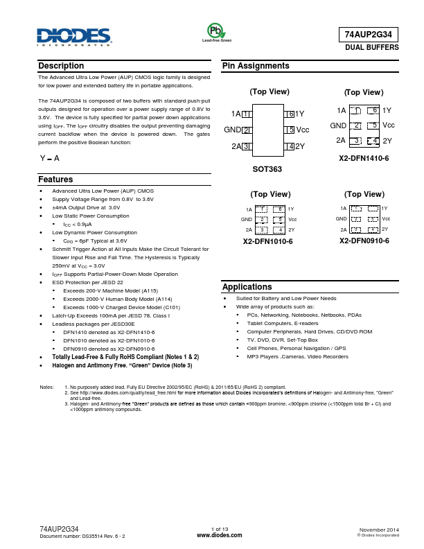
Pin Assignments
(Top View)
1A 1 GND 2
2A 3
6 ...