DM74LS20 Dual 4-Input NAND Gate
June 1986 Revised March 2000
DM74LS20 Dual 4-Input NAND Gate
General Description
This ...
DM74LS20 Dual 4-Input NAND Gate
June 1986 Revised March 2000
DM74LS20 Dual 4-Input NAND Gate
General Description
This device contains two independent gates each of which performs the logic NAND function.
Ordering Code:
Order Number DM74LS20M DM74LS20N Package Number M14A N14A Package Description 14-Lead Small Outline Integrated Circuit (SOIC), JEDEC MS-120, 0.150 Narrow 14-Lead Plastic Dual-In-Line Package (PDIP), JEDEC MS-001, 0.300 Wide
Devices also available in Tape and Reel. Specify by appending the suffix letter “X” to the ordering code.
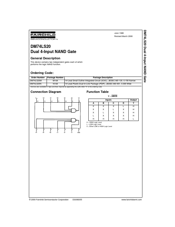
Connection Diagram
Function Table
Y = ABCD Inputs A X X X L H B X X L X H C X L X X H D L X X X H Output Y H H H H L
H = HIGH Logic Level L = LOW Logic Level X = Either LOW or HIGH Logic Level
© 2000 Fairchild Semiconductor Corporation
DS006355
www.fairchildsemi.com
DM74LS20
Absolute Maximum Ratings(Note 1)
Supply
Voltage Input
Voltage Operating Free Air Temperature Range Storage Temperature Range 7V 7V 0°C to +70°C −65°C to +150°C
Note 1: The “Absolute Maximum Ratings” are those values beyond which the safety of the device cannot be guaranteed. The device should not be operated at these limits. The parametric values defined in the Electrical Characteristics tables are not guaranteed at the absolute maximum ratings. The “Recommended Operating Conditions” table will define the conditions for actual device operation.
Recommended Operating Conditions
Symbol VCC VIH VIL IOH IOL TA Supply
Voltage HIGH Level Input
Voltage LOW Leve...