74LVC2G06
DUAL INVERTERS with OPEN DRAIN OUTPUTS
Description
The 74LVC2G06 is a dual inverter gate with open drain outp...
74LVC2G06
DUAL INVERTERS with OPEN DRAIN OUTPUTS
Description
The 74LVC2G06 is a dual inverter gate with open drain outputs. The device is designed for operation with a power supply range of 1.65V to 5.5V. The input is tolerant to 5.5V allowing this device to be used in a mixed
voltage environment. The device is fully specified for partial power down applications using IOFF. The IOFF circuitry disables the output preventing damaging current backflow when the device is powered down. The open-drain output can be connected to other open drain outputs to implement active-low wired-OR or active-high wired-AND functions. The maximum sink current is 32mA.
Features
Wide Supply
Voltage Range from 1.65V to 5.5V -24mA Output Drive at 3.0V
CMOS Low Power Consumption IOFF Supports Partial-Power-Down Mode Operation Inputs Accept up to 5.5V ESD Protection Tested per JESD 22
Exceeds 200-V Machine Model (A115) Exceeds 2000-V Human Body Model (A114) Exceeds 1000-V Charged Device Model (C101) Latch-Up Exceeds 100mA per JESD 78, Class I DFN1409 package designed as a direct replacement for chip scale packaging. Range of Package Options SOT26, SOT363, X1-DFN1010-6, X2-DFN1010-6, X2-DFN1409-6, and X2-DFN1410-6 Leadless Packages Named per JESD30E Totally Lead-Free & Fully RoHS Compliant (Notes 1 & 2) Halogen and Antimony Free. “Green” Device (Note 3)
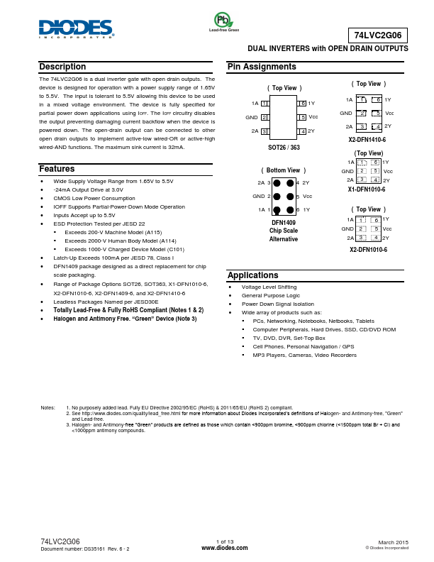
Pin Assignments
( Top View )
1A 1 GND 2
2A 3
6 1Y 5 Vcc 4 2Y
SOT26 / 363
( Bottom View )
2A 3
4 2Y
GND 2
5 Vcc
...