79M05/79M12
®
79M05/79M12
Pb Free Plating Product
Pb
1 Ampere Surface Mount Negative Three Terminal Voltage Regulato...
79M05/79M12
®
79M05/79M12
Pb Free Plating Product
Pb
1 Ampere Surface Mount Negative Three Terminal
Voltage Regulators
Features
● Output
Voltage: -5 & -12V ● Output current up to 1A ● No external components required ● Internal thermal overload protection ● Internal short-circuit current limiting ● Output transistor safe-area compensation ● Output
voltage offered in 4% tolerance
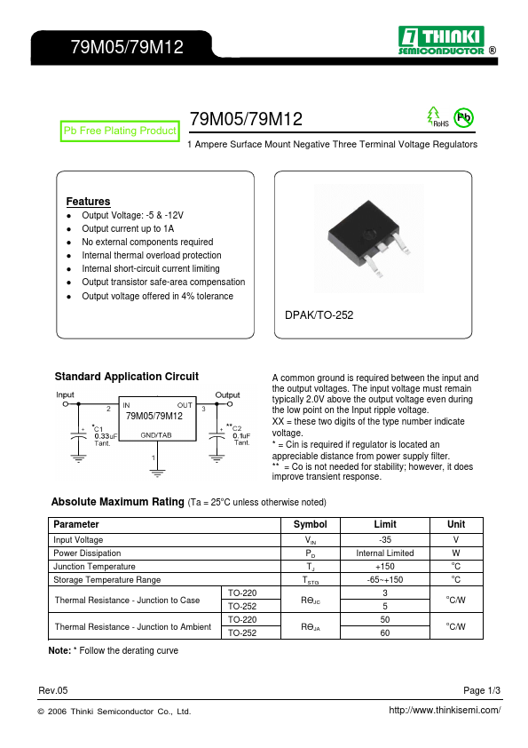
DPAK/TO-252
Standard Application Circuit
79M05/79M12
A common ground is required between the input and the output
voltages. The input
voltage must remain typically 2.0V above the output
voltage even during the low point on the Input ripple
voltage. XX = these two digits of the type number indicate
voltage.
* = Cin is required if regulator is located an
appreciable distance from power supply filter. ** = Co is not needed for stability; however, it does improve transient response.
Absolute Maximum Rating (Ta = 25oC unless otherwise noted)
Parameter
Input
Voltage Power Dissipation Junction Temperature Storage Temperature Range Thermal Resistance - Junction to Case
Thermal Resistance - Junction to Ambient
Note: * Follow the derating curve
TO-220 TO-252 TO-220 TO-252
Symbol
VIN PD TJ TSTG
RӨJC
RӨJA
Limit
-35 Internal Limited
+150 -65~+150
3 5 50 60
Unit
V W oC oC
oC/W
oC/W
Rev.05 © 2006 Thinki Semiconductor Co., Ltd.
Page 1/3 http://www.thinkisemi.com/
79M05/79M12
®
79M05 ElectricalCharacteristics
(Vin= -10V, Iout=500mA, 0oC≤Tj≤125oC, Cin=0.33uF, Cout=0.1uF; unless otherwise specified.)
...