SEMICONDUCTOR
TECHNICAL DATA
General Description
This planar stripe MOSFET has better characteristics, such as fast sw...
SEMICONDUCTOR
TECHNICAL DATA
General Description
This planar stripe
MOSFET has better characteristics, such as fast switching time, low on resistance, low gate charge and excellent avalanche characteristics. It is mainly suitable for active power factor correction and switching mode power supplies.
FEATURES VDSS=650V, ID=7A Drain-Source ON Resistance : RDS(ON)=1.4 @VGS=10V Qg(typ.)= 32nC
wwMwA.DXaItMaSUheMetR4UA.cToImNG (Tc=25 )
CHARACTERISTIC
RATING
SYMBOL
KHB7D0N65F1 UNIT
KHB7D0N65P1
KHB7D0N65F2
Drain-Source
Voltage Gate-Source
Voltage
VDSS VGSS
650 V 30 V
@TC=25
Drain Current @TC=100
Pulsed (Note1)
Single Pulsed Avalanche Energy (Note 2) Repetitive Avalanche Energy (Note 1) Peak Diode Recovery dv/dt (Note 3)
Drain Power Dissipation
Tc=25 Derate above 25
Maximum Junction Temperature
Storage Temperature Range
Thermal Characteristics
ID IDP EAS EAR dv/dt
PD Tj Tstg
7 7* 4.2 4.2* 28 28*
212
1.6
4.5 160 52 1.28 0.42
150 -55 150
A
mJ mJ V/ns W W/
Thermal Resistance, Junction-to-Case RthJC
0.78
Thermal Resistance, Case-to-Sink
RthCS
0.5
Thermal Resistance, Junction-to-Ambient
RthJA
62.5
* : Drain current limited by maximum junction temperature.
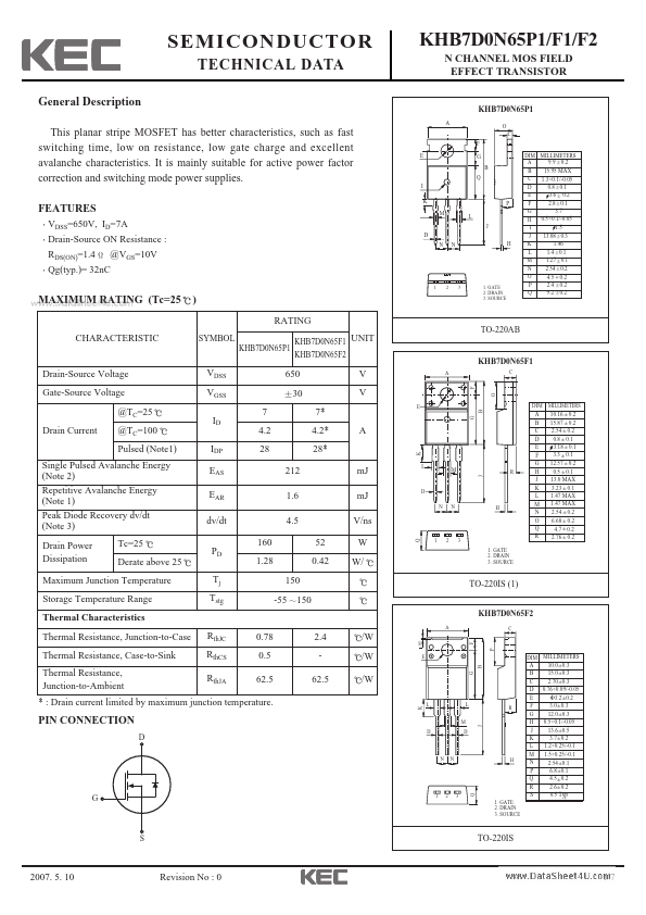
PIN CONNECTION
2.4 /W - /W
62.5 /W
D
G
2007. 5. 10
S
Revision No : 0
Q
KHB7D0N65P1/F1/F2
N CHANNEL MOS FIELD EFFECT TRANSISTOR
KHB7D0N65P1
A
E
I K
M D
NN
F G
B Q
L J
O C
P H
123
1. GATE 2. DRAIN 3. SOURCE
DIM MILLIMETERS A 9.9 +_ 0.2
B 15.95 MAX
C 1.3+0.1/-0.05 D 0.8 +_ 0.1 E 3.6 +_ 0.2 F 2.8 +_...