1. Package Outline Drawings a
Package type : P622
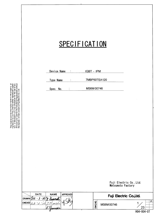
MS6M 00746
Lot No.
7MBP50TEA120
50A 1200V JAPAN O
) Notes 1.□はをす。...
1. Package Outline Drawings a
Package type : P622
MS6M 00746
Lot No.
7MBP50TEA120
50A 1200V JAPAN O
) Notes 1.□はをす。
"□" means theoretical dimensions. 2.ピッチはとする。
The dimensions of the terminals are defined at the bottom. 3.( )は、とする。
The dimensions in ( ) means referential values.
Indication of Lot No.
Odered No. in monthly Manufactured month (Jan.~Sep.:1~9,Oct.:O,Nov.:N,Dec.:D) Last digit of manufactured year
Dimensions in mm
3 23
H04-004-03
a
2. Pin Descriptions Main circuit Symbol P U V W N B
Description Positive input supply
voltage. Output (U). Output (V). Output (W). Negative input supply
voltage. Collector terminal of Brake IGBT.
Control circuit No. 1 2 3 4
Symbol
Description
GNDU High side ground (U).
ALMU Alarm signal output (U).
VinU Logic input for IGBT gate drive (U).
VccU High side supply
voltage (U).
5 GNDV High side ground (V). 6 ALMV Alarm signal output (V). 7 VinV Logic input for IGBT gate drive (V). 8 VccV High side supply
voltage (V).
9 GNDW High side ground (W). 10 ALMW Alarm signal output (W). 11 VinW Logic input for IGBT gate drive (W). 12 VccW High side supply
voltage (W).
13 GND Low side ground. 14 Vcc Low side supply
voltage. 15 VinDB Logic input for Brake IGBT gate drive. 16 VinX Logic input for IGBT gate drive (X). 17 VinY Logic input for IGBT gate drive (Y). 18 VinZ Logic input for IGBT gate drive (Z). 19 ALM Low side alarm signal output.
MS6M 00746
4 23
a
H04-004-03
3. Block Diagram
VccU 4 VinU 3 ALMU 2
GNDU 1
RALM 1.5k
...