2.5V LVDS 1:16 Clock Fanout Buffer
8T349316
DATASHEET
General Description
The 8T349316 is a 2.5V differential clock b...
2.5V LVDS 1:16 Clock Fanout Buffer
8T349316
DATASHEET
General Description
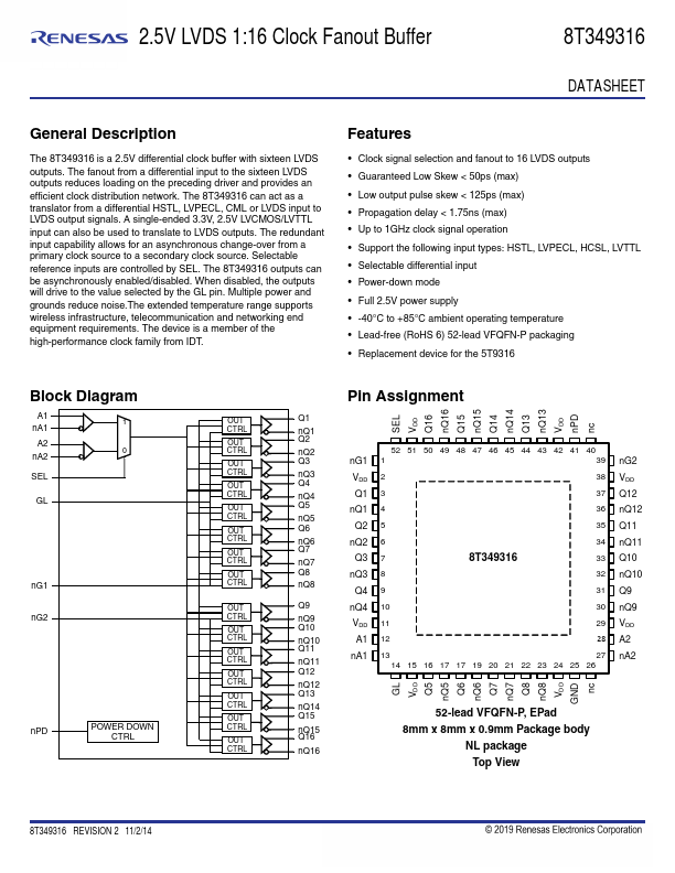
The 8T349316 is a 2.5V differential clock buffer with sixteen LVDS outputs. The fanout from a differential input to the sixteen LVDS outputs reduces loading on the preceding driver and provides an efficient clock distribution network. The 8T349316 can act as a translator from a differential HSTL, LVPECL, CML or LVDS input to LVDS output signals. A single-ended 3.3V, 2.5V LV
CMOS/LVTTL input can also be used to translate to LVDS outputs. The redundant input capability allows for an asynchronous change-over from a primary clock source to a secondary clock source. Selectable reference inputs are controlled by SEL. The 8T349316 outputs can be asynchronously enabled/disabled. When disabled, the outputs will drive to the value selected by the GL pin. Multiple power and grounds reduce noise.The extended temperature range supports wireless infrastructure, telecommunication and networking end equipment requirements. The device is a member of the high-performance clock family from IDT.
Features
Clock signal selection and fanout to 16 LVDS outputs Guaranteed Low Skew < 50ps (max) Low output pulse skew < 125ps (max) Propagation delay < 1.75ns (max) Up to 1GHz clock signal operation Support the following input types: HSTL, LVPECL, HCSL, LVTTL Selectable differential input Power-down mode Full 2.5V power supply -40°C to +85°C ambient operating temperature Lead-free (RoHS 6) 52-lead VFQFN-P pa...