SEMICONDUCTOR
TECHNICAL DATA
General Description
KHB9D5N20P1/F1/F2
www.DataSheet4U.com
N CHANNEL MOS FIELD EFFECT TRAN...
SEMICONDUCTOR
TECHNICAL DATA
General Description
KHB9D5N20P1/F1/F2
www.DataSheet4U.com
N CHANNEL MOS FIELD EFFECT TRANSISTOR
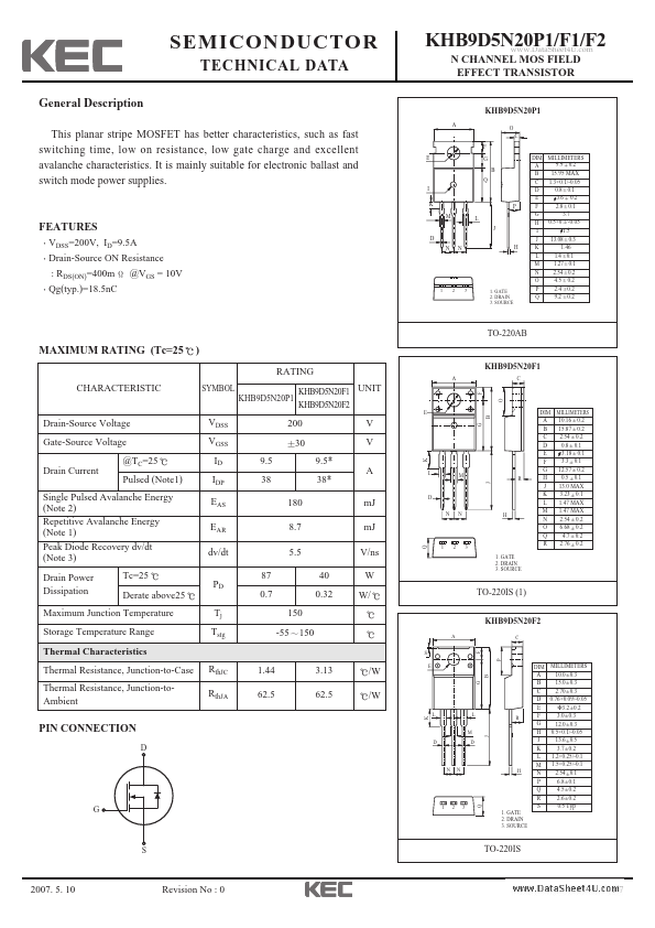
KHB9D5N20P1
A O C F E G B Q I K M L J D N N H P
DIM MILLIMETERS _ 0.2 9.9 + A B C D E F G H I J K L M N O
1 2 3
This planar stripe
MOSFET has better characteristics, such as fast switching time, low on resistance, low gate charge and excellent avalanche characteristics. It is mainly suitable for electronic ballast and switch mode power supplies.
FEATURES
VDSS=200V, ID=9.5A Drain-Source ON Resistance : RDS(ON)=400m Qg(typ.)=18.5nC @VGS = 10V
15.95 MAX 1.3+0.1/-0.05 _ 0.1 0.8 + _ 0.2 3.6 + _ 0.1 2.8 + 3.7 0.5+0.1/-0.05 1.5 _ 0.3 13.08 + 1.46 _ 0.1 1.4 + _ 0.1 1.27 + _ 0.2 2.54 + _ 4.5 + 0.2 _ 0.2 2.4 + _ 0.2 9.2 +
1. GATE 2. DRAIN 3. SOURCE
P Q
TO-220AB
MAXIMUM RATING (Tc=25
)
RATING
A F
KHB9D5N20F1
C
CHARACTERISTIC
SYMBOL
KHB9D5N20F1 UNIT KHB9D5N20P1 KHB9D5N20F2
E
O
DIM
B
MILLIMETERS
Drain-Source
Voltage Gate-Source
Voltage Drain Current @TC=25 Pulsed (Note1) Single Pulsed Avalanche Energy (Note 2) Repetitive Avalanche Energy (Note 1) Peak Diode Recovery dv/dt (Note 3) Drain Power Dissipation Tc=25 Derate above25
VDSS VGSS ID IDP EAS EAR dv/dt 87 PD 0.7 Tj Tstg 9.5 38
200 30 9.5*
V V A 38*
K
L
M J
R
180 8.7 5.5 40 0.32 150 -55 150
mJ mJ
Q
D N N
H
V/ns W W/
1
2
3
A B C D E F G H J K L M N O Q R
_ 0.2 10.16 + _ 0.2 15.87 + _ 0.2 2.54 + _ 0.1 0.8 + _ 0.1 3.18 + _ 0.1 3.3 + _ 12.57 + 0.2 _ 0.1 0.5 + 13.0 MAX _ 0.1 3.23 + 1....