12-Output Differential Buffer
12-Output Differential Buffer for PCIe Gen3
9DB1233 Datasheet
Description
The 9DB1233 zero-delay buffer supports PCIe ...
Description
12-Output Differential Buffer for PCIe Gen3
9DB1233 Datasheet
Description
The 9DB1233 zero-delay buffer supports PCIe Gen3 requirements, while being backwards compatible to PCIe Gen2 and Gen1. The 9DB1233 is driven by a differential SRC output pair from an IDT 932S421 or 932SQ420 or equivalent main clock generator. It attenuates jitter on the input clock and has a selectable PLL bandwidth to maximize performance in systems with or without spread-spectrum clocking.
Typical Applications
▪ 12-output PCIe Gen3 zero-delay/fanout buffer
Output Features
▪ Twelve 0.7V current mode differential HSCL output pairs
Features
▪ 3 selectable SMBus addresses; multiple devices can share the same SMBus segment
▪ 12 OE# pins; hardware control of each output ▪ PLL or bypass mode; PLL can dejitter incoming clock ▪ Selectable PLL bandwidth; minimizes jitter peaking in
downstream PLLs ▪ Spread spectrum compatible; tracks spreading input clock for
low EMI ▪ SMBus interface; unused outputs can be disabled ▪ Undriven differential outputs in Power-down; improved power
management
Key Specifications
▪ Cycle-to-cycle jitter < 50ps ▪ Output-to-output skew < 50ps ▪ PCIe Gen3 phase jitter < 1.0ps RMS ▪ Pin compatible with DB1200 Yellow Cover device
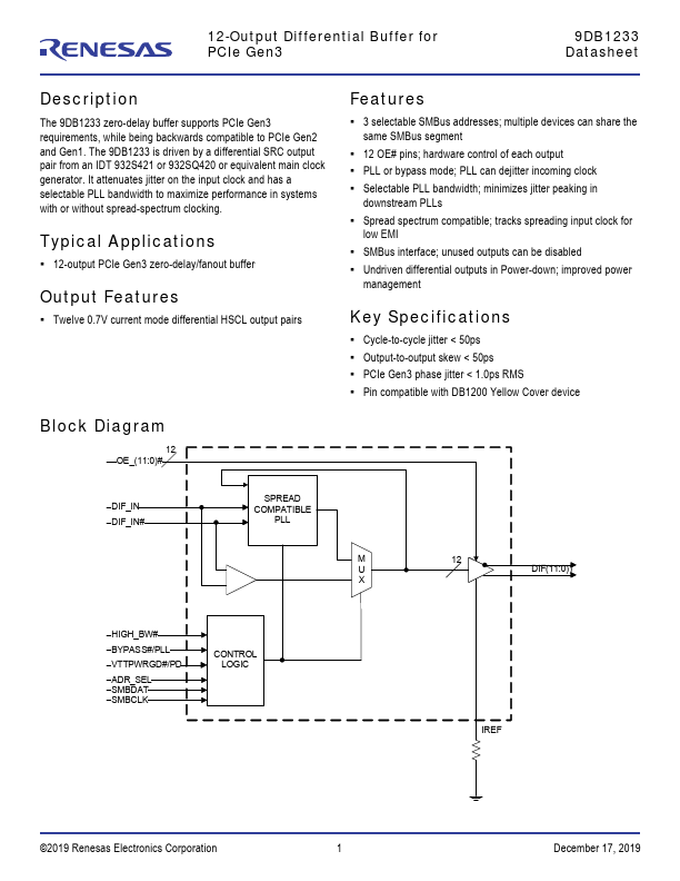
Block Diagram
12 OE_(11:0)#
DIF_IN DIF_IN#
SPREAD COMPATIBLE
PLL
M 12 U DIF(11:0)) X
HIGH_BW# BYPASS#/PLL VTTPWRGD#/PD ADR_SEL SMBDAT SMBCLK
CONTROL LOGIC
IREF
©2019 Renesas Electronics Corporation
1
December 17, 2019
9DB1233 Datasheet
Contents
Descr...
Similar Datasheet