Nineteen Output Differential Buffer
Nineteen Output Differential Buffer for PCIe Gen3
DATASHEET
9DB1933
Recommended Application
19 output PCIe Gen3 zero-d...
Description
Nineteen Output Differential Buffer for PCIe Gen3
DATASHEET
9DB1933
Recommended Application
19 output PCIe Gen3 zero-delay/fanout buffer
General Description
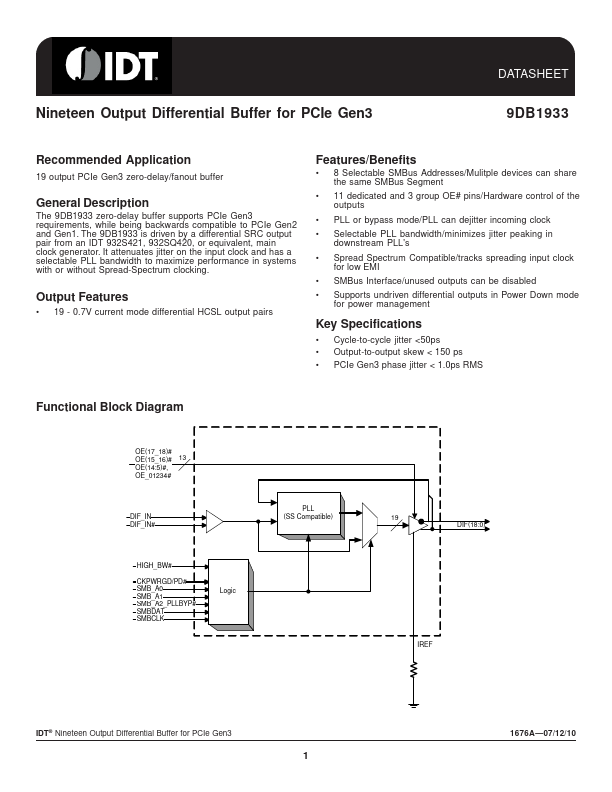
The 9DB1933 zero-delay buffer supports PCIe Gen3 requirements, while being backwards compatible to PCIe Gen2 and Gen1. The 9DB1933 is driven by a differential SRC output pair from an IDT 932S421, 932SQ420, or equivalent, main clock generator. It attenuates jitter on the input clock and has a selectable PLL bandwidth to maximize performance in systems with or without Spread-Spectrum clocking.
Output Features
19 - 0.7V current mode differential HCSL output pairs
Features/Benefits
8 Selectable SMBus Addresses/Mulitple devices can share the same SMBus Segment
11 dedicated and 3 group OE# pins/Hardware control of the outputs
PLL or bypass mode/PLL can dejitter incoming clock
Selectable PLL bandwidth/minimizes jitter peaking in downstream PLL's
Spread Spectrum Compatible/tracks spreading input clock for low EMI...
Similar Datasheet