2-Output 3.3V LP-HCSL Zero-Delay Buffer
2-Output 3.3V LP-HCSL Zero-Delay 9DBL0243 / 9DBL0253
Buffer with LOS Indicator
Datasheet
Description
The 9DBL0243 / 9...
Description
2-Output 3.3V LP-HCSL Zero-Delay 9DBL0243 / 9DBL0253
Buffer with LOS Indicator
Datasheet
Description
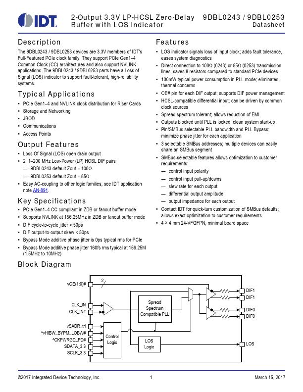
The 9DBL0243 / 9DBL0253 devices are 3.3V members of IDT's Full-Featured PCIe clock family. They support PCIe Gen1–4 Common Clock (CC) architectures and also support NVLINK applications. The 9DBL0243 / 9DBL0253 parts have a Loss of Signal (LOS) indicator to support fault-tolerant, high-reliability systems.
Typical Applications
▪ PCIe Gen1–4 and NVLINK clock distribution for Riser Cards ▪ Storage and Networking ▪ JBOD ▪ Communications ▪ Access Points
Output Features
▪ Loss Of Signal (LOS) open drain output ▪ 2 1–200 MHz Low-Power (LP) HCSL DIF pairs
— 9DBL0243 default Zout = 100Ω — 9DBL0253 default Zout = 85Ω ▪ Easy AC-coupling to other logic families; see IDT application note AN-891.
Key Specifications
▪ PCIe Gen1–4 CC compliant in ZDB or fanout buffer mode ▪ Supports NVLINK at 156.25MHz in ZDB or fanout buffer mode ▪ DIF cycle-to-cycle jitter < 5...
Similar Datasheet