2-output 1.8V PCIe Gen1/2/3 Zero Delay / Fanout Buffer
2-output 1.8V PCIe Gen1/2/3 Zero Delay / Fanout Buffer
9DBV0231
DATASHEET
Description
The 9DBV0231 is a member of IDT'...
Description
2-output 1.8V PCIe Gen1/2/3 Zero Delay / Fanout Buffer
9DBV0231
DATASHEET
Description
The 9DBV0231 is a member of IDT's 1.8V Very-Low-Power (VLP) PCIe family. The device has 2 output enables for clock management.
Recommended Application
1.8V PCIe Gen1/2/3 Zero-Delay/Fan-out Buffer (ZDB/FOB)
Output Features
2 – 1-200MHz Low-Power (LP) HCSL DIF pairs
Key Specifications
DIF cycle-to-cycle jitter <50ps DIF output-to-output skew <50ps DIF additive phase jitter is <100fs rms for PCIe Gen3 DIF additive phase jitter <300fs rms (12k-20MHz)
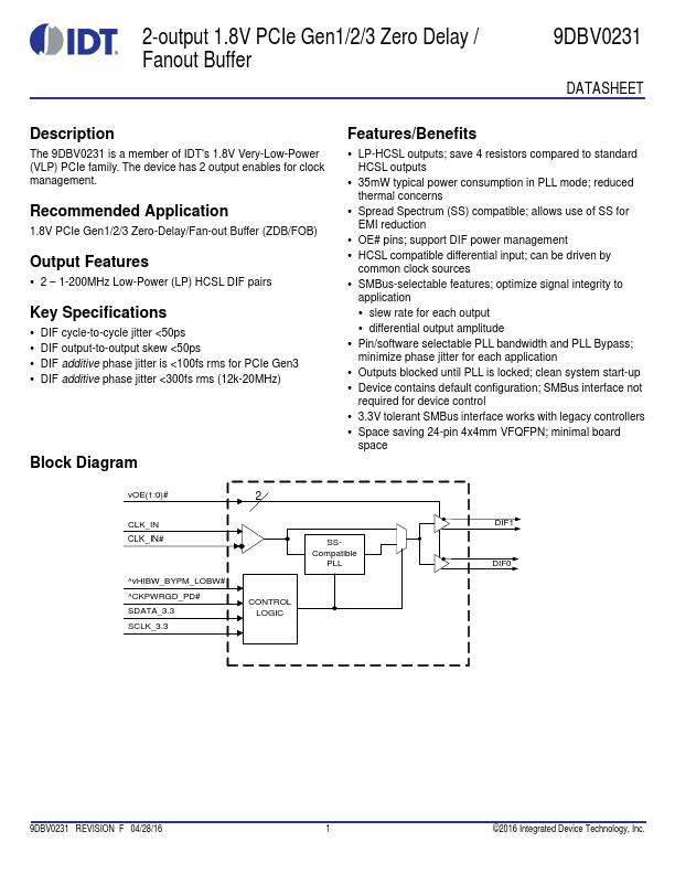
Block Diagram
Features/Benefits
LP-HCSL outputs; save 4 resistors compared to standard
HCSL outputs
35mW typical power consumption in PLL mode; reduced
thermal concerns
Spread Spectrum (SS) compatible; allows use of SS for
EMI reduction
OE# pins; support DIF power management HCSL compatible differential input; can be driven by
common clock sources
SMBus-selectable features; optimize signal integrity to
applicat...
Similar Datasheet