2:1 1.5V PCIe Gen1-2-3 Clock Mux
2:1 1.5V PCIe Gen1-2-3 Clock Mux w/Zo=100ohms
9DMU0141
DATASHEET
General Description
The 9DMU0141 is a member of IDT's...
Description
2:1 1.5V PCIe Gen1-2-3 Clock Mux w/Zo=100ohms
9DMU0141
DATASHEET
General Description
The 9DMU0141 is a member of IDT's SOC-Friendly 1.5V Ultra-Low-Power (ULP) PCIe Gen1-2-3 family. It has integrated output terminations providing Zo=100ohms for direct connection to 100ohm transmission lines. The output has an OE# pin for optimal system control and power management. The part provides asynchronous or glitch-free switching modes.
Recommended Application
2:1 1.5V PCIe Gen1-2-3 Clock Mux
Output Features
1 – Low-Power (LP) HCSL DIF pair w/Zo=100
Key Specifications
DIF additive cycle-to-cycle jitter <5ps DIF phase jitter is PCIe Gen1-2-3 compliant 125MHz additive phase jitter 535fs rms typical (12kHz to
20MHz)
Features/Benefits
LP-HCSL output w/integrated terminations; saves 4
resistors compared to standard HCSL output
1.5V operation; 11mW typical power consumption Selectable asynchronous or glitch-free switching; allows
the mux to be selected at power up even if both inputs are not running, then transition to glitch-free switching mode
Spread Spectrum Compatible; supports EMI reduction OE# pins; support DIF power management HCSL differential inputs; can be driven by common clock
sources
1MHz to 167MHz operating frequency Space saving 16-pin 3x3mm VFQFPN; minimal board
space
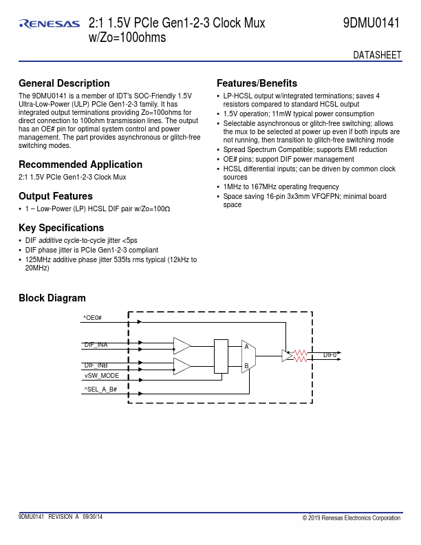
Block Diagram
^OE0#
DIF_INA
DIF_INB vSW_MODE ^SEL_A_B#
A DIF0
B
9DMU0141 REVISION A 09/30/14
1
©2014 Integrated Device Technology, Inc.
9DMU0141 DATASHEET
Pin Configuration
DIF...
Similar Datasheet