6-output 3.3V PCIe Clock Generator
9FGL06
DATASHEET
Description
The 9FGL06 devices are 3.3V members of IDT's 3.3V Ful...
6-output 3.3V PCIe Clock Generator
9FGL06
DATASHEET
Description
The 9FGL06 devices are 3.3V members of IDT's 3.3V Full-Featured PCIe family. The devices have 6 output enables for clock management and support 2 different spread spectrum levels in addition to spread off. The 9FGL06 supports PCIe Gen1-4 Common Clocked architectures (CC) and PCIe Separate Reference no-Spread (SRnS) and Separate Reference Independent Spread (SRIS) clocking architectures. The 9FGL06P1 can be programmed with a user-defined power up default SMBus configuration.
Recommended Application
PCIe Gen1-4 clock generation for Riser Cards, Storage, Networking, JBOD, Communications, Access Points
Output Features
6 – 100 MHz Low-Power HCSL (LP-HCSL) DIF pairs 9FGL0641 default ZOUT = 100 9FGL0651 default ZOUT = 85 9FGL06P1 factory programmable defaults
1 - 3.3V LV
CMOS REF output w/Wake-On-LAN (WOL)
support
Easy AC-coupling to other logic families, see IDT
application note AN-891
Key Specifications
PCIe Gen1-2-3-4 CC-compliant PCIe Gen2-3 SRIS-compliant DIF cycle-to-cycle jitter <50ps DIF output-to-output skew <50ps DIF 12k-20M phase jitter is <2ps rms when SSC is off REF phase jitter is <300fs rms, SSC off, and <1.5ps rms,
SSC is On
±100ppm frequency accuracy on all clocks
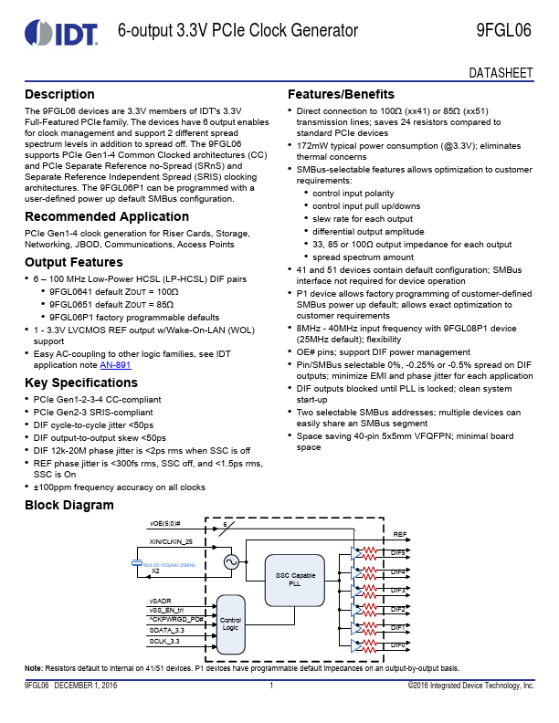
Block Diagram
Features/Benefits
Direct connection to 100 (xx41) or 85 (xx51)
transmission lines; saves 24 resistors compared to standard PCIe devices
172mW typical power consumption (@3.3V); eliminates
ther...