4 to 12-Output Buffers
4 to 12-Output Buffers for PCIe Gen1–5 and UPI
9ZXL04x1E/9ZXL06x1E/ 9ZXL08x1E/9ZXL12x1E
Datasheet
Description
The 9ZXL...
Description
4 to 12-Output Buffers for PCIe Gen1–5 and UPI
9ZXL04x1E/9ZXL06x1E/ 9ZXL08x1E/9ZXL12x1E
Datasheet
Description
The 9ZXL04x1E/9ZXL06x1E/9ZXL08x1E/9ZXL12x1E family of Zero-Delay/Fanout Buffers (ZDB, FOB) are 2nd-generation enhanced performance buffers for PCIe and CPU applications. The family meets all published QPI/UPI, DB2000Q and PCIe Gen1–5 jitter specifications. Devices range from 4 to 12 outputs, with each output having an OE# pin to support the PCIe CLKREQ# function for low power states. All devices meet DB2000Q, DB1200ZL and DB800ZL jitter and skew requirements.
PCIe Clocking Architectures
▪ Common Clocked (CC) ▪ Independent Reference (IR) with and without spread spectrum
(SRIS, SRNS)
Key Specifications
▪ Fanout Buffer Mode additive phase jitter:
PCIe Gen5 CC < 24fs RMS DB2000Q additive jitter < 40fs RMS QPI/UPI 11.4GB/s < 40fs RMS IF-UPI additive jitter < 70fs RMS
▪ ZDB Mode phase jitter:
PCIe Gen5 CC < 22fs RMS QPI/UPI 11.4GB/s < 120fs RMS IF-UPI additive jitter < 130fs RMS
▪ Cycle-to-cycle jitter < 50ps ▪ Output-to-output skew < 50 ps
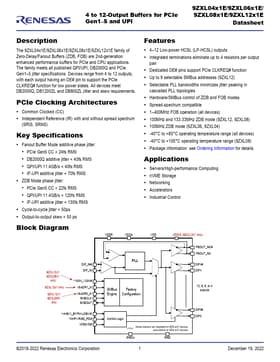
Block Diagram
VDDR
VDDA
Features
▪ 4–12 Low-power HCSL (LP-HCSL) outputs ▪ Integrated terminations eliminate up to 4 resistors per output
pair ▪ Dedicated OE# pins support PCIe CLKREQ# function ▪ Up to 9 selectable SMBus addresses (9ZXL12) ▪ Selectable PLL bandwidths minimizes jitter peaking in
cascaded PLL topologies ▪ Hardware/SMBus control of ZDB and FOB modes ▪ Spread-spectrum compatible ▪ 1–400MHz FOB operation...
Similar Datasheet