DATA SHEET
MOS FIELD EFFECT TRANSISTOR
µ PA1757
SWITCHING N-CHANNEL POWER MOS FET INDUSTRIAL USE
Description
This pr...
DATA SHEET
MOS FIELD EFFECT TRANSISTOR
µ PA1757
SWITCHING N-CHANNEL POWER MOS FET INDUSTRIAL USE
Description
This product is Dual N-Channel MOS Field Effect Transistor
www.DataSheet4U.com
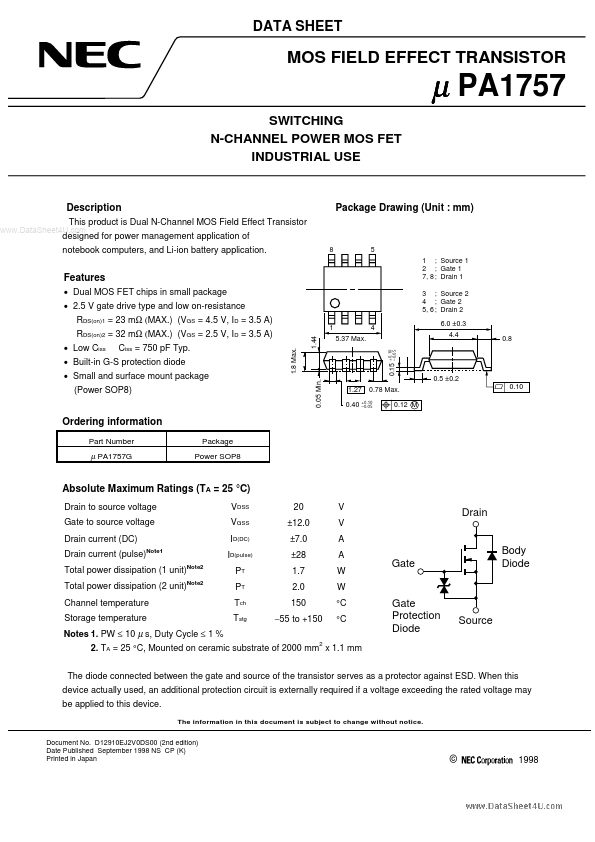
Package Drawing (Unit : mm)
designed for power management application of notebook computers, and Li-ion battery application.
8 5 1 ; Source 1 2 ; Gate 1 7, 8 ; Drain 1 3 ; Source 2 4 ; Gate 2 5, 6 ; Drain 2 1 4 5.37 Max.
+0.10 –0.05
Features
Dual MOS FET chips in small package 2.5 V gate drive type and low on-resistance RDS(on)1 = 23 mΩ (MAX.) (VGS = 4.5 V, ID = 3.5 A)
1.44
6.0 ±0.3 4.4 0.8
RDS(on)2 = 32 mΩ (MAX.) (VGS = 2.5 V, ID = 3.5 A) Built-in G-S protection diode Small and surface mount package (Power SOP8)
1.8 Max.
Low Ciss
Ciss = 750 pF Typ.
0.15
0.05 Min.
0.5 ±0.2 0.10
1.27 0.40
0.78 Max. 0.12 M
+0.10 –0.05
Ordering information
Part Number Package Power SOP8
µ PA1757G
Absolute Maximum Ratings (TA = 25 °C)
Drain to source
voltage Gate to source
voltage Drain current (DC) Drain current (pulse)
Note1 Note2 Note2
VDSS VGSS ID(DC) ID(pulse) PT PT Tch Tstg
20 ±12.0 ±7.0 ±28 1.7 2.0 150 −55 to +150
2
V V A A W W °C °C
Drain
Total power dissipation (1 unit) Total power dissipation (2 unit) Channel temperature Storage temperature
Gate
Body Diode
Notes 1. PW ≤ 10 µ s, Duty Cycle ≤ 1 % 2. TA = 25 °C, Mounted on ceramic substrate of 2000 mm x 1.1 mm
Gate Protection Diode
Source
The diode connected between the gate and source of the transistor serves as a...