ACE1512E
N-Channel Enhancement Mode Field Effect Transistor with ESD Protection
Description The ACE1512E uses advanced ...
ACE1512E
N-Channel Enhancement Mode Field Effect Transistor with ESD Protection
Description The ACE1512E uses advanced trench technology to provide excellent RDS(ON) and low gate charge. They offer operation over a wide gate drive range from 1.8V to 8V. It is ESD protected.
Features
VDS (V)=20V ID=6.5A (VGS=4.5V) RDS(ON)<21mΩ (VGS=4.5V) RDS(ON)<25mΩ (VGS=2.5V) RDS(ON)<33mΩ (VGS=1.8V) ESD Protected : 2000V
Absolute Maximum Ratings
Parameter
Drain-Source
Voltage
Gate-Source
Voltage
Drain Current (Continuous)*AC TA=25℃ TA=70℃
Drain Current (Pulsed)*B
Power Dissipation
TA=25℃ TA=70℃
Operating temperature / storage temperature
Symbol Ratings Unit
VDSS 20 V
VGSS ±8 V
6.5
ID
A 5.2
IDM 24 A
1
PD
W 0.64
TJ/TSTG -55~150 ℃
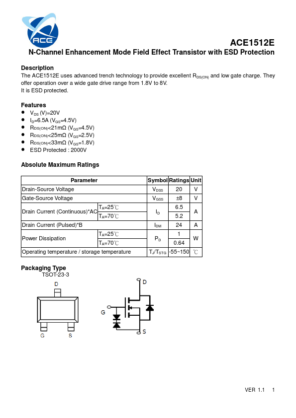
Packaging Type TSOT-23-3
VER 1.1 1
ACE1512E
N-Channel Enhancement Mode Field Effect Transistor with ESD Protection
Ordering information ACE1512EBMS + H
Halogen - free
Pb - free
BMS : TSOT-23-3
Electrical Characteristics
TA=25℃, unless otherwise specified.
Parameter
Drain-source breakdown
voltage Zero gate
voltage drain current
Gate threshold
voltage Gate leakage current
Drain-source on-state resistance
Forward transconductance Diode forward
voltage
Maximum body-diode continuous current
Total gate charge Gate-source charge Gate-drain charge Turn-on delay time
Turn-on rise time Turn-off delay time
Turn-off fall time
Input capacitance Output capacitance Reverse transfer capacitance
Note :
Symbol
Test Conditions
Min Typ Max Unit...