ACE1526B
P-Channel Enhancement Mode Field Effect Transistor
Description ACE1526B uses advanced trench technology to pro...
ACE1526B
P-Channel Enhancement Mode Field Effect Transistor
Description ACE1526B uses advanced trench technology to provide excellent RDS(ON). This device particularly suits for low
voltage application such as power management of desktop computer or notebook computer power management, DC/DC converter.
Features VDS (V) = -30V ID = -6A (VGS = -10V) RDS(ON) < 75mΩ (VGS = -10V) RDS(ON) < 80mΩ (VGS = -4.5V)
Absolute Maximum Ratings Parameter
Drain-Source
Voltage Gate-Source
Voltage
Drain Current (Continuous) *AC Drain Current (Pulse) *B
TA=25°C TA=70°C
Power Dissipation
TA=25°C TA=70°C
Operating Temperature/ Storage Temperature
Symbol VDSS VGSS
ID
IDM PD
TJ//TSTG
Max -30 ±20 -6 -4.8 -30 50 25 -55~150
Unit V V
A
A W ℃
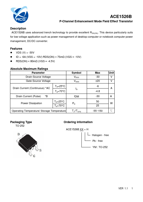
Packaging Type TO-252
Ordering information
ACE1526B XX + H Halogen - free Pb - free YM : TO-252
VER 1.1 1
ACE1526B
P-Channel Enhancement Mode Field Effect Transistor
Electrical CharacteristicsTA=25℃, unless otherwise specified.
Parameter
Symbol
Conditions
Static
Drain-Source Breakdown
Voltage
V(BR)DSS
VGS=0V, ID=250uA
Zero Gate
Voltage Drain Current
IDSS
VDS=-30V, VGS=0V
Gate Threshold
Voltage Gate Leakage Current
VGS(th) IGSS
VGS=VGS, IDS=-250uA VGS=±20V, VDS=0V
Drain-Source On-Resistance
Forward Transconductance
RDS(ON) gFS
VGS=-10V, ID=-6A VGS=-4.5V, ID=-3A
VDS=-10V,ID=-5.3A
Diode Forward
Voltage
VSD
IS=-1.7A, VGS=0V Switching
Min. Typ. Max. Unit
-30 V
-1 uA
-1 -1.4
55 68
-6 V 100 nA 75 mΩ 80
10 S
-0.82 -1.2
V
Tota...