a
+2.5 V to +5.5 V, 230 A Dual Rail-to-Rail, Voltage Output 8-/10-/12-Bit DACs AD5302/AD5312/AD5322*
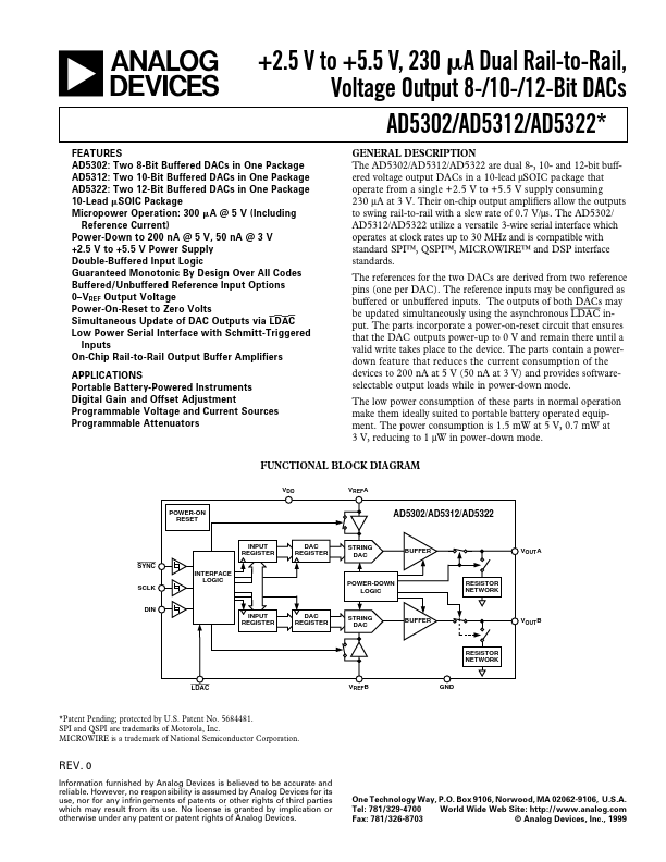
GENERAL DESCRIPTI...
a
+2.5 V to +5.5 V, 230 A Dual Rail-to-Rail,
Voltage Output 8-/10-/12-Bit DACs AD5302/AD5312/AD5322*
GENERAL DESCRIPTION
FEATURES AD5302: Two 8-Bit Buffered DACs in One Package AD5312: Two 10-Bit Buffered DACs in One Package AD5322: Two 12-Bit Buffered DACs in One Package 10-Lead SOIC Package Micropower Operation: 300 A @ 5 V (Including Reference Current) Power-Down to 200 nA @ 5 V, 50 nA @ 3 V +2.5 V to +5.5 V Power Supply Double-Buffered Input Logic Guaranteed Monotonic By Design Over All Codes Buffered/Unbuffered Reference Input Options 0–V REF Output
Voltage Power-On-Reset to Zero Volts Simultaneous Update of DAC Outputs via LDAC Low Power Serial Interface with Schmitt-Triggered Inputs On-Chip Rail-to-Rail Output Buffer
Amplifiers APPLICATIONS Portable Battery-Powered Instruments Digital Gain and Offset Adjustment Programmable
Voltage and Current Sources Programmable Attenuators
The AD5302/AD5312/AD5322 are dual 8-, 10- and 12-bit buffered
voltage output DACs in a 10-lead µSOIC package that operate from a single +2.5 V to +5.5 V supply consuming 230 µA at 3 V. Their on-chip output
amplifiers allow the outputs to swing rail-to-rail with a slew rate of 0.7 V/µs. The AD5302/ AD5312/AD5322 utilize a versatile 3-wire serial interface which operates at clock rates up to 30 MHz and is compatible with standard SPI™, QSPI™, MICROWIRE™ and DSP interface standards. The references for the two DACs are derived from two reference pins (one per DAC). The reference inputs may be c...